Microcontrollers of the AVR family from Atmel. Atmel marking: Atmel non-volatile memory chips with serial interface
Federal Agency for Railway Transport
Far Eastern State Transport University
Department of "Telecommunications"
course project
By discipline: "Microprocessor information management systems"
On the subject: "AVR family microcontrollers from Atmel"
Khabarovsk
Introduction
A classic microprocessor system uses a separate processor chip, separate memory chips, and separate input/output ports. The rapid development of microprocessor technology requires more and more more microchip integration.
That is why microcircuits were developed that combine all the elements of a microprocessor system at once. Such microprocessors are called microcontrollers. AT Soviet time such microcircuits were called "single-chip microcomputers".
For single-chip microcontrollers, the concept of "central processing unit" is usually not used. Since the processor is still a separate device. The functions of the processor in the microcontroller are replaced by an arithmetic logic unit (ALU).
In addition to the ALU, the microcontroller contains:
♦ clock generator;
♦ data memory;
♦ program memory;
♦ I/O ports.
All these elements are interconnected by internal data and address buses. The microcontroller communicates with the outside world using I / O ports. Any microcontroller always has one or more ports. In addition, modern microcontrollers always have a built-in interrupt system, as well as built-in programmable timers, comparators, digital-to-analog converters, and much more.
If we are not talking about a large computer, but about a portable control device, then microcontrollers are used in it. Of course, any real circuit rarely does without simple logic circuits, flip-flops, counters, and the like. But the basis is always the microcontroller. Pure microprocessors are currently used only in personal computers.
1. Atmel microcontroller ATtiny2313/V
1.1 Structure, main characteristics and capabilities
The ATtiny 2313 is an 8-bit microcontroller with 2KB internal programmable Flash memory.
♦ uses AVRRISC architecture;
♦AVR is high speed and special low power RISC architecture;
♦ 120 powerful instructions, most of which are executed in one machine cycle;
♦ 32 eight-bit general-purpose registers;
♦ completely static organization (minimum frequency can be 0);
♦ up to 20 million operations per second (MIPS/Sec) at 20 MHz.
Saving programs and data when the power is off:
♦ 2 KB of built-in programmable Flash-memory, up to 10,000 write/erase cycles;
♦ 128 bytes of built-in programmable non-volatile data memory (EEPROM);
♦ up to 10,000 write/erase cycles;
♦ 128 bytes of internal RAM (SRAM);
♦ programmable read/write protection bits for program memory and EEPROM.
Peripherals:
♦ one 8-bit timer/counter with programmable determinant and match mode;
♦ one 16-bit timer/counter with programmable determinant, match mode, and capture mode;
♦ four channels of PWM (PWM);
♦ built-in analog comparator;
♦ programmable watchdog timer and built-in clock generator;
♦ universal serial interface USI (Universal Serial Interface);
♦ full duplex USART.
Features of the microcontroller:
♦ special input debug WIRE to control the built-in debugging system;
♦ in-system programmable serial interface SPI;
♦ support for both external and internal interrupt sources;
♦ three low consumption modes (Idle, Power-down and Standby);
♦ built-in system of hardware reset at power on;
♦ internal tunable clock generator;
♦ I/O circuits and housing;
♦ 18 programmable I/O lines;
♦ three types of hulls;
PDIP - 20 contacts;
SOIC - 20 pins;
QFN/MLF - 20 pads.
Supply voltage:
♦ 1.8 - 5.5V (for ATtiny2313V);
♦ 2.7 - 5.5V (for ATtiny2313).
ATtiny2313V Clock Generator Frequency Range:
♦ 0-4 MHz at 1.8-5.5 V;
♦ 0-10 MHz at 2.7-5.5 V.
ATtiny2313 clock generator frequency range:
♦ 0-10MHz at 2.7-5.5V;
♦ 0-20 MHz at 4.5-5.5 V.
Current consumption in active mode:
♦ 1 MHz, 1.8 V: 230 µA;
♦ 32 kHz, 1.8 V: 20 µA (with internal oscillator).
Current consumption in low consumption mode:
♦ no more than 0.1 μA at a voltage of 1.8 V.
Microcontroller Block Diagram
The pin assignment of the ATtiny2313 chip is shown in fig. 1. The block diagram of the ATtiny2313 microcontroller is shown in fig. 2.
The AVR core has a large instruction set for working with 32 general purpose registers. All 32 registers are directly connected to the arithmetic logic unit (ALU), which allows you to execute an instruction for two different registers in one cycle of the system clock. This architecture has made it possible to achieve performance ten times greater than that of traditional microcontrollers built using CISC technology.
Rice. 1 - ATtiny2313 pin assignments
1.2 Features of the ATtiny2313 chip
The ATtiny2313 chip has the following features:
♦ 2 Kbytes of system programmable Flash program memory;
♦ 128 bytes EEPROM;
♦ 128 bytes SRAM (RAM);
♦ 18 input-output lines (I/O);
♦ 32 working registers;
♦ one-wire interface for in-circuit debugging;
♦ two multifunctional timers/counters with matching function;
♦ support for external and internal interrupts;
♦ serial programmable USART port;

Rice. 2 - Block diagram of the microcontroller ATtiny2313
♦ universal serial interface with a transmission start detector;
♦ programmable watchdog timer with internal generator;
♦ three programmable power saving modes.
In Idle mode, the central processor is suspended, the rest of the systems continue to work. Exit from this mode is possible both by external interruption and by internal one. For example, when the timer overflows.
In PowerDown mode, the contents of the registers are preserved, but the operation of the internal generator is suspended and all other functions of the microcircuit are disabled. The mode can be exited by an external interrupt or after a system reset. This solution allows you to combine a quick start with low power consumption.
The microcircuit is manufactured using Atmel's unique high-frequency technology. The internal Flash program memory can be reprogrammed using the ISP interface without removing the microcontroller from the board. Combining an 8-bit RISC processor with in-system reprogrammable Flash memory on a single chip makes the ATtiny2313 chip powerful tool, which provides very flexible and low cost solutions to many control applications.
In my course project, some part of the microcontroller will be described.
2. Central core of the processor
The main function of the central core of the processor is to control the process of executing programs. To do this, the CPU must have direct access to memory, must be able to perform all kinds of calculations and execute interrupt requests.
Consider the general issues of AVR architecture.
2.1 Brief description of the architecture
To maximize speed and enable parallel execution of several operations, AVR microcontrollers use the Havard architecture (Fig. 3).

Rice. 3 - AVR Architecture Block Diagram
This architecture provides separate memory and a separate address bus for both program and data.
Each instruction of five programs is executed in one machine cycle using multi-level pipeline processing. At the moment when the next instruction is executed, the next instruction is read from the program memory. This concept allows you to execute one instruction per clock cycle of the system generator. The program memory segment is physically a built-in reprogrammable Flash memory.
The fast access register file contains 32 eight-bit general-purpose registers, which are accessed in one cycle of the system clock. This allows the Arithmetic Logic Unit (OLU) to perform most of its operations in a single clock cycle.
A typical ALU operation is performed as follows: two operands are read from the register file, the operation is performed. The result of saving is again in the register file. All three of these actions are performed in one cycle of the clock generator.
Six of the 32 registers can be used as three 16-bit indirect pointer registers. These dual registers can be used to address data in the RAM address space. Such an organization makes it possible to programmatically calculate the address.
One of these pointer registers can also be used as a pointer to the address of data located in program memory (Flash memory). These additional compound 16-bit registers are referred to as X, Y, and Z.
The ALU supports arithmetic and logical operations between two registrars or between a constant and a registrar. The ALU can also perform operations on individual registrars. After each arithmetic operation, the status register is updated to reflect information about its result.
The sequence of program execution can be changed by conditional and unconditional branch instructions, as well as by the subroutine call instruction, which use direct addressing.
Most AVR instructions are one 16-bit word. Each program memory address contains a 16-bit instruction or half of a 32-bit instruction.
When an interrupt routine or subroutine is executed, the current value of the program counter (PC) is stored on the stack.
The stack is actually located in the same address space as the SRAM data memory (RAM) and, therefore, the size of the stack is limited only by the size of the SRAM and how much of the SRAM is used by the rest of the program.
The user program must always initialize the stack pointer (SP) immediately after reset (before a subroutine is executed or an interrupt is called). The stack pointer (SP) has its specific address in the I/O register space. Data in RAM (SRAM) can be accessed using memory different ways addressing supported by the AVR architecture.
The address space of all types of memory in the AVR architecture is regular linear. The flexible interrupt module has a number of control registers in the I/O register address space and an additional global interrupt enable flag in the status register.
Each type of interrupt has its own vector in the interrupt vector table. Interrupts are prioritized according to their position in the interrupt vector table. The lower the interrupt vector address, the higher the priority.
The I/O register space contains 64 addresses for peripheral device control registers, processor mode control registers, and other I/O functions. Any I/O register can be accessed directly by its number or as a data memory location. In the data memory address space, the I/O registers are located immediately after the general purpose register file (0x20 - 0x5F).
2.2 ALU - Arithmetic Logic Unit
The high performance ALU operates in direct communication with all 32 general purpose registers. In one cycle of the clock generator, an arithmetic operation is performed between two RONs or between RONs and a directly specified constant. All ALU operations are divided into three main categories:
♦ arithmetic;
♦ logical;
♦ operations with digits.
A feature of the architecture is that when performing arithmetic operations, all operands can be considered both unsigned and signed numbers.
Status register
The status register contains information about the results of the last arithmetic or logic instruction. This information can be used to change the flow of program execution in conditional jump instructions and other conditional statements.
When an interrupt routine is called, the status register is not automatically saved. The programmer must provide instructions in the interrupt handling procedure that will save the contents of this register at the beginning and restore it at the end. Note that the status register cannot be directly placed on the stack. First, you will have to save one of the general-purpose registers on the stack, then put the contents of the status register into the vacated register, and then move the information from this intermediate register to the stack.
General purpose register file
The register file is optimized for the AVRRISC instruction set. In order to achieve the required performance and flexibility, the register file supports the following I/O schemes:
♦ output of one 8-bit operand and input of one 8-bit result of calculations;
♦ output of two 8-bit operands and input of one 8-bit calculation result;
♦ output of two 8-bit operands and input of one 16-bit calculation result;
♦Output one 16-bit operand and input one 16-bit result.
On fig. 4 shows the structure of 32 general purpose registers used as working registers of the microcontroller.

Rice. 4 - General purpose register file for AVR microcontrollers
Most instructions that operate on a register file have direct access to all of its registers, and most of them execute in a single clock cycle.
As shown in fig. 5, each register also has an address in the data memory space where they occupy the first 32 locations. Although the registers are not physically part of the SRAM, this memory organization provides more flexibility when accessing the registers. The indirect memory access pointer (one of the X, Y, or Z registers) can be set to any register in the file.
2.3 X-register, Y-register and Z-register
Registers R26-R31, in addition to their main purpose, have an additional function. These registers can serve as 16-bit address pointers for operations using indirect addressing. The three indirect address registers X, Y, and Z are defined as shown in Fig. 5.
In various instructions using indirect addressing, these registers can be used as permanent address sources, as an address register with automatic address increment, and as an address register with automatic address decrement.

Rice. 5 - Dual registers X, Y, Z
stack pointer
The stack is mainly used:
♦ for temporary data storage;
♦ for storing local variables;
♦ to store the exit address of a subroutine or interrupt routine.
The stack pointer register always points to the top of the stack.
The stack pointer points to a stack area in data memory (SRAM). On the stack, among other things, are stored;
♦ subroutine exit address;
♦ exit address from the interrupt routine.
Therefore, in any program, the address of the beginning of the stack must be determined before any subroutine is called and before interrupts are enabled. Initially, the stack pointer must be set to an address no lower than 0x60.
The stack pointer is decremented by one when data is pushed onto the stack with the PUSH instruction, and decremented by two when data is pushed onto the stack at the return address from a subroutine or interrupt routine.
The stack pointer is incremented by one when data is read from the stack with the POP instruction, and incremented by two when data is popped from the stack on exit from a subroutine (RET instruction) or completion of an interrupt routine (RETI instruction).
The stack pointer in all AVR chips is made in the form of two 8-bit I / O registers. The number of bits actually used for each microcontroller model is different. In some models, including the ATtiny2313, the amount of data memory is so small that only the lowest stack pointer (SPL) register is used for the stack pointer. They do not have an SPH register. The structure of the stack pointer registers for the ATtiny2313 microcontroller is shown below.
Memory ATtiny2313
Now consider different kinds ATtiny2313 microcontroller memory. The AVR architecture contains two main types of memory:
♦ data memory;
♦ program memory.
In addition, the ATtiny2313 has an EEPROM for long-term data storage. All three types of memory are contiguous areas with linearly increasing addresses.
2.4 System Flash Program Memory
The ATtiny2313 chip contains 2KB of on-chip FRAM for program storage. Since all instructions used in the AVR are 16 or 32 bits in size, the program memory is organized as 1Rx 16. Graphically, the program memory address space is shown in Fig. 6.

Rice. 6 - Program memory card
The program memory allows at least 10,000 write/erase cycles. The ATtiny2313's program counter (PC) has 10 bits and can therefore handle a 1K address space. The microcircuit supports the low program memory programming mode, which can be carried out via the serial SPI interface.
In the program memory, you can also place any data that remains unchanged during the operation of the program. The LPM instruction is used to retrieve this data from program memory.
2.5 SRAM data memory
On fig. Figure 6 shows the organization of data memory - RAM (SRAM) of the ATtiny 2313 microcontroller. In total, the RAM address space contains 224 cells that are occupied:
♦ general purpose register file;
♦ additional input-output registers;
♦ internal data memory.
The first 32 cells are aligned with the RON file. The next 64 cells are the standard area where all I/O registers are located. And only the remaining 128 cells make up the internal data memory.
There are five different ways addressing for data memory:
♦ straight;
♦ indirect with offset;
♦ indirect;
♦ indirect with pre-decrement;
♦ indirect with postincrement.
Registers R26-R31 (X, Y, Z) serve as address pointers for all indirect addressing operations.
With direct addressing, the full address of the data byte is specified.
With offset indirection, 63 locations can be covered, starting at the current base address pointed to by the contents of the Y or Z register.
When using indirect addressing with automatic pre-decrement and automatic post-decrement, after reading (writing) the memory, the address written to the X, Y or Z register is changed.
All 32 general purpose registers, 64 I/O registers, and 128 bytes of ATtiny2313 SRAM data memory are available for all memory addressing options.
EEPROM data memory
The ATtiny2313 chip contains 128 bytes of EEPROM memory. It is organized as a separate address space for storing data, in which each byte can be individually read or written.
The exchange of data between the EEPROM and the CPU is described below and takes place using:
♦ EEPROM address register;
♦ data register EEPROM;
♦ EEPROM control register.
EEPROM Read/Write Process
The registers used to access the EEPROM are normal I/O registers. The presence of the auto-detect readiness time function allows the user program to independently determine the moment when the next byte can be written. If the program contains instructions that write to EEPROM, some precautions must be taken.
In power circuits equipped with a good filter, the VCC voltage will change slowly when turned on and off. This causes the device to operate for some time at a lower voltage than the minimum allowable voltage for a given clock frequency.
3. I/O ports
All ports on AVR microcontrollers in digital I/O mode are full-fledged bidirectional ports, in which each of the pins can work both in input mode and in output mode. This means that each individual port bit can be configured as either an input or an output, regardless of the configuration of all other bits on the same port.
The port bits can be configured using the reset and set SBI and CBI commands. The same goes for changing the output value (if the bit is configured as an output) or turning on/off the internal load resistor (if the bit is configured as an input).
All these settings are made separately for each port pin. The output buffer of each port pin contains a high-capacity, balanced output stage. The load capacity of each pin of any port is sufficient to drive the LED display directly.
All pins of any port have individually connected load resistors, which can be connected between this pin and the power supply if necessary. The input circuits of each port line have two protection diodes connected to the power circuit and to the common wire, as shown in fig. 7.
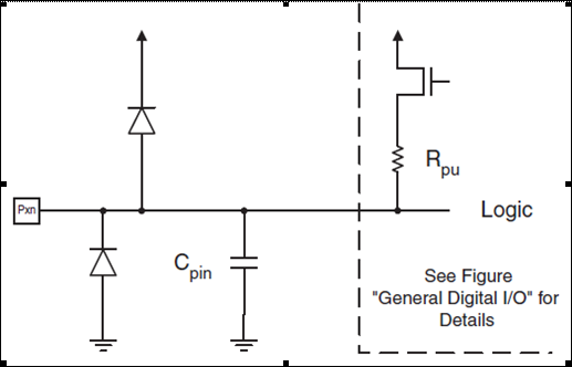
Rice. 7 - Equivalent circuit of the input circuits of one bit of the I / O port
The letter “x” in the description of the register names means the name of the port, the lowercase letter “n” means the bit number. When using this name in a program, instead of these characters, you need to substitute a specific letter of the port name and a specific bit number.
For example, PORTB3 is for bit number 3 of port B, if this bit was called PORTxn in the documentation.
There are three special registers for each I/O port in the microcontroller:
♦ PORTx – data register;
♦ DDRx – control register;
♦ PINx – register for direct reading of the state of the port lines.
The direct read port line status register is read-only, while the data register and control register are both read and write.
However, it is also possible to write a logical unit to any bit of the PINx register. It will cause the corresponding bit of the data register (PORTx) to toggle. Each bit in the PORTx register controls whether the internal terminating resistor is enabled or disabled when the corresponding port bit is in input mode.
3.1 Using Ports for Digital I/O
Each bit of the port is a bidirectional I/O line with the ability to connect the internal load resistance. On fig. 8 is a functional diagram of one line of an I/O port. The output pin of this line is labeled Pxn in the diagram.

Rice. 8 - Simplified diagram of one line of digital I / O
Pin configuration
Each bit of the port is associated with three bits of three special registers: DDxn; PORTxn; PINxn.
As already stated:
♦ bit DDxn is bit number n of the DDRx register;
♦ bit PORTxn is bit number n of register PORTx;
♦ The PINxn bit is bit number n of the PINx register.
The DDxn bit of the DDRx register selects the direction of information transfer of the corresponding bit. If a logical one is written to DDxn, the Pxn bit works as an output. If a logical zero is written to DDxn, the Pxn bit works as an input.
If the port bit is configured as an input, setting the PORTxn bit to one enables the internal load resistor. To disable the load resistor, you need a logical zero in PORTxn. Immediately after a system reset, all pins of all ports go into the third (high impedance) state.
If the port bit is configured as an output (setting the PORTxn bit to one), then that one will appear at the output of the port. If a logical zero is written to the PORTxn bit, then the output will be zero.
4. External interrupts
4.1 Purpose and modes of operation
To call external interrupts, use the inputs INT0, INT1 or any of the PCINT7-0 inputs. If interrupts are enabled, they will be triggered even if the INT0, INT1 and PCINT7-0 pins are configured as outputs.
This feature provides the ability to generate interrupts programmatically. The PCI1 interrupt is a signal change interrupt on any of the PCINT7-8 pins. The PCI0 interrupt is an interrupt on a change in any PCINT7-0 signal. Moreover, both for the PCI1 interrupt and for the PCI0 interrupt, any of the inputs assigned to it can be arbitrarily excluded from operation.
The PCMSK1 and PCMSK0 control registers determine which inputs will trigger the corresponding interrupt. The change interrupt on the PCINT7-0 pins works in an asynchronous manner. That's why this species interrupts can be used to wake up from all sleep modes except Idle mode.
Interrupts INT0 and INT1 support several modes. They can be triggered on a rising edge, a falling edge, or a static low logic signal. The choice of one of these modes is made using the external interrupt control register - EICRA.
When one of the interrupts INT0 or INT1 is enabled and configured as a low input, an interrupt request will be generated as long as the input is low.
Calling interrupts INT0 and INT1 at a low level is carried out in asynchronous mode. This means that such an interrupt can be used to wake up from any sleep mode except Idle.
The startup time of the microcontroller is determined using the SUT and CKSEL fuse switches.
5. Eight-digit timer/counter with PWM mode support
5.1 Purpose and features
The T0 timer/counter is a versatile 8-bit counter module with two independent matching modules and PWM support. It allows you to generate specified time intervals (for real-time operation). It can also serve as a periodic signal generator.
Consider the main characteristics of the timer / counter.
5.2 Simplified block diagram
A simplified block diagram of an eight-bit timer/counter is shown in fig. 9. Registers available for the central core and data transfer circuits are shown in bold lines in the diagram.

Rice. 9 - Block diagram of an 8-bit timer/counter
5.3 Registers
Both the timer/counter counter register (TCNT0) and both match registers (OCR0A and OCR0B) are eight-bit registers. The presence of an interrupt request (in Fig. 10 it is abbreviated as “interrupt call.”) can always be determined by the state of the corresponding interrupt flag in the TIFR register.
Each interrupt can be individually masked using the TIMSK timer interrupt mask register. The TIFR and TIMSK registers in fig. 9 are not shown.
The timer/counter can operate both from an internal clock generator through a prescaler, and from an external clock signal fed to input T0. The clock source select circuit passes the selected clock source to the timer/counter input, and each pulse of this signal increments (or decrements) its value.
If none of the clock sources is selected, the timer/counter stops.
The signal at the output of the clock source selection circuit (clkT0) is called the timer clock signal.
The contents of the OCR0A and OCR0B registers are constantly compared with the timer/counter value. The result of the comparison can be used by the generator to generate a PWM signal or a variable frequency square wave on one of the OC0A or OC0B outputs.
At the time of a match, the corresponding flag OCF0A or OCF0B is set in one of the channels, which can be used to generate an interrupt request on a match.
5.4 Symbols used
When describing counters, special designations are used for all its important states. These designations are given in table. one.
Symbols for the basic states of an 8-bit counter
Table 1
5.5 Counting module
The heart of the eight-bit timer/counter is a programmable reversible counter module. On fig. 10 shows a block diagram of the counting module and its control signals.

Rice. 10 - Block diagram of the counting module
Consider internal signals:
♦ count - increments or decrements the contents of TCNT0 by 1;
♦ direction – choice between decrease and increase;
♦ clear – clear TCNT0 (set all bits to zero);
♦ clkT0 – clock frequency of the timer/counter;
♦ top - occurs when TCNT0 is reached maximum value;
♦ bottom – occurs when TCNT0 reaches the minimum value (zero).
Depending on the timer mode, each clock pulse (clkT0) clears, increments, or decrements the counter. clkT0 signal can be received from both external and internal source clock signal. This is determined by the clock select bits (CS02:0). When no clock source is selected (CS02:0 = 0), the timer stops.
The CPU can access the value of the TCNT0 register whether the clkT0 signal is present or not. The write command from the CPU takes precedence over all other operations (counter clear or count operations).
The timer modes are determined by setting bits WGM01 and WGM00 in register TCCR0A and bit WGM02 in register TCCR0B. There is a close relationship between the selected meter operation mode and the signal frequency at the OC0A output.
The Timer/Counter Overflow Flag (TOV0) is set according to the mode of operation selected with the WGM01:0 bits. The TOV0 flag can be used to generate CPU interrupts.
5.6 Match module
The heart of the module is an eight-bit comparator that continuously compares the contents of the TCNT0 register with the contents of each of the two match registers (OCR0A or OCR0B). Each time the content of TCNT0 is equal to the content of OCR0A or OCR0B, the comparator generates a match signal. This signal sets the corresponding match flag (OCF0A or OCF0B) on the next clock cycle.
If the corresponding interrupt is enabled, setting the match flag causes the interrupt. The match flag is automatically cleared when the interrupt routine is started. The flag can also be cleared programmatically by writing a logical one to it.
In the frequency generator mode, the match signal is used to generate the match output signal is used to generate the output signal according to the selected operating mode, which is determined by the WGM02:0 bits as well as the compare mode select bits (COM0x 1:0). The max and bottom signals are used by the frequency generator in some cases to obtain critical values in individual modes work. On fig. 11 shows a block diagram of a match module. In the figure, the letter x is symbol. For different moduli of coincidence, x is either A or B.

Rice. 11 - Block diagram of the match module
The OCR0x registers are double buffered in any Pulse Width Modulation (PWM) mode. In Normal mode and CTC (Clear on Coincidence) mode, double buffering is disabled. Double buffering synchronizes the update of the OCR0x register with the timer reaching the upper or lower limits. Synchronization prevents the occurrence of asymmetric PWM pulses, that is, pulses whose length is equal to an odd number of cycles. This ensures high quality PWM signals.
Accessing the OCR0x register may seem too complicated. Actually it is not. If double buffering is enabled, the CPU accesses the OCR0x registers through the buffer. If buffering is disabled, the CPU accesses the OCR0x registers directly.
5.7 Force change of match output state
In all non-PWM timer modes, the signal on any of the match outputs can be forced to change by writing a one to the special FOC0x bit. Forcing a match output change does not set the OCF0x flag and does not reset the timer.
The signal at the OC0x output will change in the same way as in a real match. That is, the behavior of the OC0x output will depend on the setting of the COM0x1:0 bits. Depending on the value of these bits, the output signal will either be set to one, or reset to zero, or change its value to the opposite.
5.8 Blocking the match mode at the time of writing the TCNT0 register
When a value is written to the TCNT0 register, the compare operation is blocked for one clock of the timer input signal. This happens even if the timer is stopped. This feature allows the OCR0x register to be written to the same value as the TCNT0 register without triggering an interrupt when the timer/counter clock is input.
5.9 Using the interrupt module
As already mentioned, in any mode of the timer, at the time of writing the TCNT0 register, the operation of the comparison module is suspended for one period of the clock signal. This can lead to errors when changing the contents of the TCNT0 register, regardless of whether the timer/counter is running or not.
If the value written to TCNT0 is equal to the value written to OCR0x, the compare operation will be skipped, which will cause the timer to malfunction in frequency generator mode.
For the same reason, you cannot write a value equal to BOTTOM to TCNT0 when the counter is in countdown mode.
The OC0x output operating modes must be configured before the corresponding port line can be configured as an output. The easiest way to install desired value on OC0x output – use forced setting (FOC0x bit) in Normal mode. The OC0x registers retain their value when switching signal generation modes.
5.10 Coincidence signal output module
Bits COM0x1:0 perform two functions. The frequency generator uses the COM0x1:0 bits to determine how the output of the match module (OC0x) will change when a match is detected. At the same time, the COM0x1:0 bits control the signal source at the OC0x output.
On fig. Figure 12 shows a simplified diagram showing the logic behind the operation of the COM0x1:0 bits.

Rice. 12 - Coincidence signal output circuit
As can be seen from the figure, the value COM0x1:0 affects the state of the input/output port of the microcircuit, regardless of the main control registers for this port (DDR and PORT). And when we talk about the status of OC0x, you need to understand that the internal register OC0x is not the same as the contact of the OC0x microcircuit. Immediately after a system reset, zero is written to the OC0x register.
If any of the COM0x1:0 bits is set, then the main function of the I/O port is canceled and the match signal (OC0x) from the frequency generator is passed to the output. At the same time, the direction of information transfer of the OC0x pin (input or output) still depends on the corresponding bit of the DDR register.
The value of the bit that determines the direction of information transfer for the OC0x pin, if it is to work as an output, must be set before the value of the OC0x register is sent to this output. Alternate port functions are independent of the signal generator's operating mode.
5.11 Operating modes
The mode of operation, that is, the behavior of the timer/counter and match signal output, is determined by both the signal generator's mode of operation (WGM02:0) and the match signal output mode (COM0x1:0). The state of the bits that determine the output mode of the match signal does not affect the counting sequence, which is determined only by the state of the signal generator configuration bits.
The COM0x1:0 bits determine whether the PWM output should be inverted or not (inverted or non-inverted PWM). For non-PWM modes, the content of the COM0x1:0 bits determines whether the output signal should be set to one, reset to zero, or switched to the opposite state at the time of the match.
5.12 Normal mode
The Normal mode (WGM02:0 = 0) is the simplest of the timer modes. In this mode, the counting direction is always forward (the contents increase), and the counter is not forced to reset. The counter simply overflows when it reaches a maximum of eight bits (TOP = 0xFF) and then restarts again (0x00).
During normal operation, the Timer/Counter Overflow Flag (TOV0) will be set when TCNT0 becomes zero. The TOV0 flag in this case behaves like the ninth bit, and then with the exception that it is only set, not cleared.
Using a timer overflow interrupt that automatically clears the TOV0 flag, you can increase the program recalculation factor by. The Normal mode doesn't have any features worth focusing on. The new value of the counting register can be written at any time.
The match module can sometimes be used to trigger interrupts. Using the coincidence signal to generate signals in Normal mode is not recommended, as this will greatly slow down the processor.
5.13 Coincidence Reset Mode (CTC)
In reset on match mode, or alternatively CTC mode (when WGM02:0 = 2), the OCR0A register is used to control the counter's conversion factor. In CTC mode, the counter is reset to zero when the contents of the register counter (TCNT0) and the OCR0A register match.
The OCR0A register thus determines the maximum value for the counter, and hence its conversion factor.
This mode allows maximum control of the signal frequency at the output of the module. The calculation of external events is also simplified. The value of the register counter (TCNT0) is incremented until a match occurs between TCNT0 and OCR0A, and then the contents of the counter (TCNT0) are cleared.
An interrupt can be called every time the counter reaches the TOP value. This uses the OCF0A flag. If the interrupt is enabled, an interrupt routine is called that can be used to update the value of TOP.
Setting TOP too close to the BOTTOM value when the counter is idle or when the prescale factor is low must be done with care, as the CTC mode does not have double buffering.
If the new value written to OCR0A is lower than the current value of TCNT0, then the source will skip the match. As a result, the counter will continue counting up to its maximum value (0xFF), then go through zero, and only then the moment of coincidence will occur.
To generate an output signal in CTC mode, the OC0A output can be set to switch the output level every time a match occurs. To do this, set the match output mode bits (COM0A1:0 = 1) to the appropriate position. The value of the OC0A register will not be sent to the corresponding external port pin if it is not configured as an output. The generated signal will have a maximum frequency fOC0 = fclk_I/O/2 when zero (0x00) is written to the OCR0A register. The signal frequency can be calculated using the following equation:
where the variable N is the prescale factor (1, 8, 64, 256, or 1024).
As in Normal mode, the TOV0 flag is set each time the counter counts up to MAX and goes to zero.
5.14 FastPWM mode (fast PWM)
The microcontroller has several modes of pulse width modulation (PWM). In English it sounds like Pulse Width Modulation (PWM). Fast PWM (fastPWM) is selected when WGM02:0 = 3 or 7. In this mode, the highest frequency PWM signal is generated. Fast PWM differs from other PWM modes in that the counter generates only an age sequence to generate a signal. That is, the change in the value of the counter has the form of a sawtooth signal with a one-sided slope.
The count starts with BOTTOM and ends with TOP. After that, the counter is restarted (the BOTTOM value is set again). The TOP value is 0xFF when WGM2:0 = 3.
If WGM2:0 = 7, the TOP value is determined by the contents of the OCR0A register. In non-inverting output mode, the match signal (OC0x) is reset when the values of TCNT0 and OCR0x match and the transition to BOTTOM occurs.
In inverting mode, the output signal is set at the moment of coincidence and transition to BOTTOM. Due to the fact that the counter always works in one direction only, the signal frequency in fast PWM mode can be twice as high as in phasecorrect PWM mode, which uses a sawtooth signal with two slopes.
Due to the high output frequency, the fast PWM mode is well suited for building power control systems, for building rectifiers and digital-to-analog converters. The high frequency allows the use of external components (coils, capacitors) of small dimensions, and thus, reduces the overall cost of the system.
In fast PWM mode, the counter value is incremented until it reaches the TOP value. On the next timer clock cycle, the counter is cleared.
The Timer/Counter Overflow Flag (TOV0) is set each time the counter reaches TOP. If the interrupt is enabled, an interrupt routine is called that can be used to update the match level.
In fast PWM mode, the match module is used to generate a PWM signal on the OC0x outputs. Setting bits COM0x1:0 = 2 will generate a non-inverted PWM signal at the output. To generate an inverted PWM signal, you must set COM0x1:0 = 3. By setting bits COM0A1:0 = 1, the AC0A output signal switches to the opposite state at the moment of coincidence, provided that the WGM02 bit = 1.
This option is not available for OC0B output. The actual OC0x value will only be sent to the external chip pin if it is configured as an output.
The PWM signal is generated by setting (resetting) the OC0x register at the moment when the values of OCR0x and TCNT0 match, and resetting (setting) this register in the first clock cycle, after the counter is reset (changing its value from TOP to BOTTOM). The frequency of the PWM signal at the output can be calculated using the following expression:
The variable N is the prescale factor (1, 8, 64, 256, or 1024). Separately, it is necessary to consider several cases when generating a PWM signal, when a value close to the limit is written to the OCR0A register.
If the OCR0A register is set to BOTTOM, the output will be a short spike for every MAX + 1 timer clock.
If the MAX value is written to the OCR0A register, this will cause the output to be constantly present either high or low logic level (depending on the value of the COM0A1: 0 bits).
The output frequency in fast PWM mode (at 50% control level) can be achieved by making the OC0x register switch its logic level on every match (COM0x1:0 = 1).
The signal formed in this way will have a maximum frequency fOC0 = fclk_I/O/2 when zero is written in the OCR0A register. This feature allows you to switch the OCR0A register in the same way as in CTC mode, but still take advantage of the double buffering that is used in fast PWM mode.
5.15 PWM, phase correct (PhaseCorrectPWM)
phase correct PWM mode (WGM02:0 = 1 or 5). The PWM signal is formed with a large conversion factor and correct in phase. Phase correctness is ensured due to the operation of the counter in the sawtooth mode with a two-sided slope.
The counter periodically changes the direction of its account. First it counts from BOTTOM to TOP, then the direction of the count changes and the counter counts from TOP to BOTTOM. Then the direction of recalculation changes again, and everything repeats from the beginning.
The value of TOP is 0xFF when WGM2:0 = 1 and is determined by register OCR0A when WGM2:0 = 5.
In the non-inverting output mode, the OCR0x output signal is reset to zero when the contents of the TCNT0 and OCR0x registers match, if the counter is working in the forward direction (increasing). The value is set to one at the time of the match if the counter is decrementing.
In the inverted output mode, the picture is reversed. The double-sided tilt mode has a lower maximum output frequency than the previous case where the single-sided tilt saw is used. Due to the phase symmetry with two-sided tilt, such modes are preferred in the creation of motor control systems.
In phase correct PWM mode, the counter increments until it reaches TOP. When the counter value reaches TOP, the counting direction changes. The content of TCNT0 will be equal to TOP for one period of the timer clock. The Timer/Counter Overflow Flag (TOV0) is set each time the counter reaches BOTTOM. The interrupt flag can be used to generate an interrupt request. This interrupt will be called every time the counter reaches the BOTTOM value.
In phasecorrect PWM mode, the match module is used to generate a PWM signal at the OC0x output. By setting the bits COM0x1:0 = 3. Setting the bits COM0A0 = 1 causes the OC0A output to be inverted each time a match occurs if the WGM02 bit is set. This option is not available for OC0B output. The actual value of OC0x is only sent to the external port pin if it is configured as an output.
The PWM signal is generated by resetting (setting) OC0x at the moment when the contents of the OCR0x and TCNT0 registers match when the counter is incrementing, and is set (reset) at the moment of the match if the counter is decrementing. The PWM output frequency in phase correct PWM mode can be calculated using the following formula:
Where the variable N is the prescale factor (1, 8, 64, 256, 1024).
The extreme values of the contents of the OCR0A register when generating PWM signals in phase correct PWM mode are special cases. For non-inverting mode, writing the value BOTTOM to the OCR0A register will cause the output to go low. Writing the MAX value to OCR0A will set the output to logic one. For the inverting mode, the output signal will have opposite values.
6. Description of the command system
6.1 Command system. General information about the command system
In the AVR family, the command system for microcontrollers different types contain from 89 to 130 commands. The 2323, 2343, 2313, 4433, 8515 and 8535 microcontrollers have 118 commands in the instruction set. We will call this system of commands the base.
In table. 2.1 - 2.13 describes the operations performed by the commands of the base system, and shows the mnemonic codes of commands used when developing a program in the AVR Assembler language. The tables give continuous numbering of commands used further in the text.
The basic command system contains:
▪ 33 commands of register operations, in the course of which only general-purpose registers are used (commands No. 1-33);
▪ 26 commands addressing the address in the SRAM address space (commands Nos. 34-59);
▪ 2 commands with access to I/O registers (commands No. 60 and 61);
▪ 1 command with access to FlashROM (command No. 62);
▪ 22 instructions for operations with bits in the bits of general-purpose registers and I/O registers (commands No. 63-84);
▪ 34 program flow control commands (commands Nos. 85-118).
The instruction set of microcontrollers of the t11, t12, t15, 1200, and t28 types that do not have SRAM does not include commands with access to an address in the SRAM address space, with the exception of commands with mnemonic codes LDRd, Z (No. 40) and STZ, Rr (No. 41), which are used to access general purpose registers and I / O registers using indirect addressing. The command system of these microcontrollers also does not include 2 register operation commands (Nos. 32 and 33) and two program control commands (Nos. 86 and 88). For microcontrollers of the 1200 type, the command system also does not include a command with access to FlashROM, and for a microcontroller of the m163 type, in addition, with the presence of a hardware multiplier.
(PC)+1→STACK
(STACK) →PC
(STACK) →PC
Table 12
| № | Condition | Command mnemonic code | № | Condition | Command mnemonic code |
| 91 | I=0 | BRID k | 92 | I = 1 | BRIE k |
| 93 | T=0 | BRTC k | 94 | T=1 | BRTS k |
| 95 | H=0 | BRHCk | 96 | H=1 | BRHS k |
| 97 | S = 02.(X)+1→X | BRGE k | 98 | S=1 | BRLT k |
| 99 | V = 0 | BRVC | 100 | V = 1 | BRVS k |
| 101 | N=0 | BRPL k | 102 | N=1 | BRMI k |
| 103 | Z = 0 | BRNE k | 104 | Z = 1 | BREQ k |
| 105 | C=0 | BRCC k | 106 | C=1 | BRCS k |
| 107 | C=0 | BRSH k | 108 | C=1 | BRLO k |
| 109 | SREG.b = 0 | BRBC b, k | 110 | SREG.b = 1 | BRBS b, k |
| k= -64 - +63; b = 0 - 7 | |||||
Table 13
Table 14
| № | Operation | Command mnemonic code |
| 116 | MK → power saving mode | SLEEP |
| 117 | Restart WDT | WDR |
| 118 | Not | NOP |
6.3 Register operation commands
The group of register operations includes transfer, arithmetic and logical operations. Commands of register operations are described in Table. 2, 3 and 4 The machine codes of all register operation instructions are in the word format, instructions No. 1 - 31 are executed in one cycle, and instructions No. 32 and 33 are executed in two cycles.
Arithmetic operations - addition and subtraction - can be performed on unsigned numbers in binary code and on signed numbers in two's complement code. Unlike many other families of microcontrollers, in which subtraction is reduced to addition with a number with a changed sign (X–Y = X + (-Y)), in microcontrollers of the AVR family, subtraction is performed using a hardware binary subtractor.
When performing arithmetic and logical operations, in addition to the result code, the values of the result attributes are formed. When performing comparison operations (commands No. 18, 19 and 27), only the values of the characteristics of the result are formed.
The result flag values are represented by the state of the bits in the status register SREG (#$33F). Six result characteristics are used and named C (SREG.0), Z(SREG.1) N (SREG.2), V (SREG.3, S (SREG.4) and H (SREG.5). 2.1 - 2.3 signs, the values of which are formed during the execution of commands, are marked with a "+" sign or their name is indicated.
When performing different operations, the value of features is formed according to different rules.
Feature C takes a single value:
▪ when a carry unit appears from the most significant digit when performing an addition operation (commands Nos. 14, 15 and 32);
▪ when a loan unit appears in the senior category during the addition operation (commands No. 4, 16, 17, 18, 19, 25, 26, 27 and 33);
▪ when a unit goes beyond the bit grid when performing a shift operation (commands No. 7, 8, 9, 10 and 11).
The single value of the sign C when performing addition and subtraction operations with numbers without a sign indicates that an incorrect result of the operation was obtained due to overflow of the bit grid.
Sign Z takes a single value when a zero result of the operation is received. When performing a subtraction operation taking into account the loan (commands No. 17, 19 and 26), Z = 1, if a zero result was obtained when performing this and previous operations.
The attribute N has a value equal to the value of the most significant digit of the result code. When performing arithmetic operations on signed numbers and there is no bit grid overflow, it represents the sign of the result.
The attribute V takes on a single value if, when performing an arithmetic operation with signed numbers, an overflow of the bit grid occurred.
The sign S = NV represents the sign of the result when performing arithmetic operations with signed numbers, regardless of the overflow of the bit grid. When the bit grid overflows (V = 1), the sign of the result is opposite to the value in the most significant bit of the result code.Sign H takes a single value in the presence of a transfer unit from bit D3 to bit D4 when performing a subtraction operation and when transferring one from bit D3 to bit D4 when performing a code operation to the left.
6.4 Commands with access to the SRAM address
By commands with access to the address in the SRAM address space, operations are performed by transferring (copying) a byte between the general-purpose register and the element that corresponds to the address in the SRAM address space. Such an element can be a general register (addresses $00 to $1F), an I/O register (addresses $20 to $5F), a memory location in SRAM (addresses $60 to the maximum address in SRAM), a memory location in ERAM (addresses from maximum address in SRAM +1 to maximum address in ERAM).
Commands with access to the address in the SRAM address space are described in Table. 2.4 and 2.5.
The machine codes of commands Nos. 34 and 35 are in the “2 word” format, the machine codes of the remaining commands are in the “word” format. Commands are executed in 2 cycles, and when accessing cells in ERAM, in 3 cycles. If necessary, an additional waiting cycle can be introduced into the instruction execution cycle when accessing ERAM.
Tables 2.4 and 2.5 use the following new designations:
▪ LECHA – general purpose register, I/O register, memory cell in SRAM, memory cell in ERAM, which are accessed using address A from the SRAM address space;
▪ (YachA) – byte in YAchA;
▪X, Y, Z – a pair of general purpose registers X (R26, R27), Y (R28, R29), Z (R30, R31), respectively;
▪ (X), (Y), (Z) – a word in a pair of registers X, Y, Z, respectively;
▪ STACK – a cell that is accessed using the address stored in the stack pointer register SP;
▪ (STACK) – byte in STACK, e;
▪ (SP) – number code in the SP register.
Instructions Nos. 34 and 35 implement direct addressing. The byte address (A = k) is specified in the command code.
In commands No. 36 - 57, indirect addressing is implemented. The byte address is in a pair of registers X, Y or Z. When executing commands No. 48 - 53, the address in the pair of registers is hardware reduced by one before the transfer is performed. When executing commands No. 54 - 57, the address to which the address is made is equal to the address in the pair of registers Y or Z, increased by one q, which is indicated in the command code. The address in the register pair remains unchanged.
Instructions 58 and 59 use the code in the stack pointer register as the address code. When the microcontroller is started, the number code 0 is entered into the stack pointer register. For normal operation of the stack, it is necessary to enter the code of another number into the stack pointer register at the beginning of the program. Usually, the highest address in SRAM is used as such a number. For example, for the microcontroller type 8515, this address is the number $025F.
6.5 Commands with access to I / O registers
By commands with access to I/O registers, operations are performed by transferring (copying) a byte between the general-purpose register and the I/O register, using its number ($00 - $3F) to select the I/O register. Commands with access to I / O registers are described in Table. 6. Machine command codes are in word format. Commands are executed in one cycle.
In table. 6, the following new designations are used:
▪ PrP – I/O register with number P;
▪ (PrP) – byte in PrP register.
When writing a command mnemonic code, instead of a specific register number, its symbolic name can be used. All I/O registers have regular names. For microcontrollers of different types, I / O registers that have the same name may have different names. When writing register names in mnemocodes, instead of their number, you must use the version of the AVR-Assembler for a microcontroller of this type.
6.6 FlashROM command
On a command with an appeal to FlashROM, a byte is transferred (copied) from half of the memory cell in FlashROM to the general-purpose register R0. The command is described in Table. 2.7. The machine code of the instruction is in the word format. The command is executed in three cycles.
Before executing the command, the address corresponding to the memory location in FlashROM where the constant is stored must be multiplied by 2 and written into a pair of Z registers (Nos. $30, $31).
When multiplied by 2 (shifting the code to the left by one bit), the least significant bit of the ZL register ($30) contains the number 0. If the least significant bit is zero, a byte is selected from the lower half of the FlashROM cell. To select a byte from the upper half of the cell, it is necessary to increase the number whose code is in the Z register pair by 1 using command No. 33 with the mnemonic code ADIWR30, 1 or ADIWZL, 1.
Writing constants to FlashROM is done when programming the microcontroller.
6.7 Bit operations instructions
Bit operations commands are described in Table. 2.8 and 2.9. The machine codes of all instructions are in word format. Commands No. 65 and 66 are executed in 2 cycles, the rest of the commands - in 1 cycle.
In table. 2.8 the following new designation is used:
▪ PrP.b – bit b (b = 0 – 7) of the I/O register with number P (P = $00 - $1F (!)), bit in the PrP.b bit.
Commands Nos. 63 and 64 transfer (copy) a bit between the specified bit of the general-purpose register and bit T of the SREG register.
By commands No. 65 and 66, the specified bit of the I / O register is set to the required state (0 or 1, respectively), and by commands No. 67 and 68 - the specified bit of the SREG register.
When writing the mnemocode of commands No. 65 and 66, instead of the register number (P), its symbolic name can be indicated, and instead of the bit number (b), the symbolic name of the bit. In microcontrollers of the AVR family, the bits of many I / O registers have regular names. These names are given in the text when considering devices in which these bits are used.
In some types of microcontrollers, the bits of the same-named registers with the same names have different numbers. When using the regular names of I / O registers in the regular names of bits in them, you must use the AVR Assembler version for the microcontroller of the corresponding type.
When assigning a regular bit name, it was assumed that this bit belongs to a certain I / O register, however, in the mnemonic code of commands Nos. 65 and 66, you must specify both the name / number of the register and the name of the bit.
The required bit value (0 or 1) in the bits of the I / O registers with numbers from $20 to $3F is set using the instructions for register operations with mnemonic codes CBR (No. 29) and SBR (No. 31), respectively.
In table. 10 shows the command mnemonic codes that set the bits of the SREG register to a certain state (0 or 1) without specifying the bit number in the command mnemonic code.
6.8 Program flow control commands
The group of commands for controlling the course of the program includes commands for unconditional and conditional jumps, switching to power-saving mode, restarting the watchdog timer, and an "idle" command.
In table. 11 describes the jump unconditional (Nos. 85 and 86), unconditional jump with return (Nos. 87 and 88), return from subroutine (No. 89), and return from interrupt program (No. 90) instructions. The following new designations are used in the table:
▪ PC – command counter;
▪ (PC) – number code in the command counter;
▪ k – number increment in the command counter.
When writing a program in assembly language, in the mnemonic codes of commands No. 85 and 87, instead of the increment k, a label (symbolic address) is indicated, written before the mnemonic code of the command to be executed. The increment is calculated and placed in the instruction's machine code during assembly.
The machine codes of commands described in tab. 11 are word format. Unconditional branch commands (Nos. 85 and 86) are executed in 2 cycles, unconditional jump and return commands (Nos. 87 and 88) - in 3 cycles, return commands (Nos. 89 and 90) - in 4 cycles.
The group of conditional branch instructions is divided into two groups. In the commands of the first subgroup, one of the bits in the SREG register is used as a condition. Conditions and mnemonic codes of the commands of the first subgroup are given in Table. 12. If the condition is met, a jump is made to the address, which is formed using the increment k specified in the instruction code ((PC) + 1 +k→PC; -64 ≤k≤ 63).
If the condition is not met, it jumps to the next instruction in the program ((PC) + 1→PC).
When writing a program in assembly language, instead of the increment k, the mnemonic code of the commands indicates the label (symbolic address) written before the mnemonic code of the command to be executed if the condition is met.
The machine codes of the commands of the first subgroup have the "word" format. When the condition is met, the command is executed in 2 cycles, when the condition is met, in 1 cycle.
If the condition is not met, a transition is made to the next instruction in the program ((PC) +1→PC). If the condition is met, the transition to the execution of the command following the next one ((PC) + 1 + 1/2→PC) occurs. The increment of the number in the program counter (1 or 2) is determined by the format of the machine code of the next instruction (1 word or 2 words, respectively).
The machine codes of the conditional jump commands of the second subgroup have the word format. Commands are executed in one cycle if the condition is not met, in 2 cycles if the condition is met and the next command (K1) has the "word" format, or in 3 cycles if the condition is not met and the next command (K1) has the "2 words" format ".
Bibliography
1. Belov A.V. AVR Microcontroller Device Developer's Guide. - St. Petersburg, "Science and Technology" 2010
2. http://www.atmel.ru/
3. ATtiny 2313 Data Sheet.
4. Grebnev V.V. Atmel AVR microcontrollers. –M. "IP RadioSoft" 2002
Atmel is well known in the world and Russian markets as a manufacturer of a wide range of microcircuits containing non-volatile memory on a chip. For example, ATF16V8/20V8/22V10 and AFT15xx series PLCs contain configuration EEPROM, AT89C microcontrollers have Flash program ROM, and AVR microcontrollers use both Flash and EEPROM on the same chip. Atmel's list of microcircuits includes, for example, two-bank Flash memory that supports burst mode, as well as "layered" microcircuits, where parallel ROM, serial ROM and RAM crystals are placed in one package, but on different "layers". This article, which does not claim to be exhaustive, is devoted to Atmel ROM chips in their “pure form”.
Atmel is an innovator in the manufacture of non-volatile memory chips: it was the first to release Flash-memory chips with a programming voltage of 5 V in 1989; the world's first to produce Flash-memory for 3.3, 2.7 and 2.5 V; In 1997, Atmel Corporation was the first to offer flash memory with a serial interface. And the list goes on...
Non-volatile memory chips currently produced by Atmel have a capacity range from 1 Kbps to 256 Mbps, and 1 Gbps chips will be launched in the near future. The product portfolio includes chips with 8- and 16-bit parallel interfaces, as well as chips with two- and three-wire serial interfaces.
Chips with a parallel interface
Earlier than others, AT27 series microcircuits with an 8-bit interface were released, which were actually analogues of ROM microcircuits with ultraviolet erasure, however, Atmel's crystals were packaged in plastic cases, which significantly reduced the cost of microcircuits. The price of "cheapness" is the impossibility of re-programming. When it became necessary to update the contents of the memory chip in the system, for example, to upgrade the version, Atmel offered three series of parallel ROM chips with electrical erasure.
The AT28 series, based on EEPROM technology, has the function of independent rewriting of each byte, which leads to an increase in the area of \u200b\u200bthe crystal and, accordingly, the price of the microcircuit. In the AT29 and AT49 series, built on the basis of Falsh technology, a different approach is implemented - here it is possible to overwrite in blocks called sectors. The sector size of AT29 memory chips is smaller than those of other manufacturers, which increases the flexibility of use. The AT49 series contains several sectors with respect to big size and, as a result, has a smaller die area and the lowest unit cost. Unlike the AT28 series microcircuits, when a voltage of 12 V must be applied to it for erasing, more modern AT29 and AT49 do not require additional source voltage for erasing and reprogramming. A convenient technological solution is to organize a boot block in a memory array with separate commands to protect it from erasure. This area of memory usually contains a bootloader program, which may also include a utility that performs the function of programming the main ROM array, for example, from a serial port. This construction of the system makes it possible to modify the content of the Flash ROM without using an external programmer. The second advantage is that you can use small-sized microcircuits in TSSOP packages and refuse ROM panels.
Microcircuits of the above families are produced for three supply voltages: standard five-volt microcircuits, microcircuits for operation at a supply voltage of 3.3 V (marked with the letters LV) and 2.7 V (marked with the letters BV).
The main parameters of typical ROM chips of the AT49BV series are given in Table. one.
Table 1
* N or T - boot block to the lower or upper addresses.
Chips with a parallel interface are mainly used to store the microprocessor program, which is executed directly from ROM, if the speed of the microprocessor is relatively low, or is copied to RAM before execution, which is typical for modern microprocessors. "Parallel" ROM chips can also be used for data storage. For this, even single-use or ultraviolet-erasable microcircuits were used, and with the advent of the first Flash-ROMs, freedom came for developers of data acquisition systems.
However, microcircuits with a parallel interface also have disadvantages due to the architecture itself. To carry out write-read operations, it is necessary to work with three buses: address, data and control. If the microcontroller uses a multiplexed address-data bus, you have to install additional latch registers on the board to store the address at which the memory will be accessed in the next cycle. But even if the microcontroller has separate address and data buses, all the circuits must be “decomposed” on the printed circuit board. A 1 MB chip requires 20 address wires and 8 data wires if a byte-interface chip is used, plus control signals, which sometimes takes up a significant amount of PCB area, especially if the device being developed has increased requirements in terms of overall dimensions.
Another drawback is the increased power consumption of the device. It is known that a significant part of the electrical power consumed by the microcircuit is used by its output stages, which should provide good signal fronts when operating on an external bus with a sufficiently large capacitance. The cardinal solution to the problem is the rejection of the parallel bus in principle and the transition to serial data exchange.
Chips with a serial interface
In connection with the general desire to reduce power consumption and miniaturization of electronic devices, the use of memory chips with a serial interface has become relevant. The popularity of Atmel serial ROM chips is eloquently evidenced by the fact that the company has released more than a billion such chips. Atmel produces universal memory chips with I2C, SPI and Microware interfaces, as well as specialized configuration memory chips of the AT17 series, designed to load FPGA-type programmable logic chips. These chips can be repeatedly reprogrammed in the system. It is noteworthy that AT17 chips can be used not only to load Atmel's own FPGAs - AT6000 and AT40K, but also to load FPGAs manufactured by Xilinx and Altera. To load the latter, the AT17A family is intended, which is compatible with Altera's EPC chips by pins. It should be noted that Atmel is ahead of other companies in terms of the start of mass production of new high-capacity configuration memory chips. In particular, it was the first in the world to produce a low-voltage microcircuit with a capacity of 2 Mbit in an 8-pin planar package.
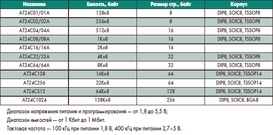
Universal serial ROM chips with a sufficient degree of conditionality can be divided into "slow" and "fast". The first category includes AT24 series microcircuits with an I 2 C interface. This two-wire interface, developed by Philips, is very convenient for exchanging small portions of data at frequencies not exceeding hundreds of kilohertz. A typical example is a household TV or computer monitor with settings memory. Chips of the AT24 series are characterized by a large number of rewriting cycles - up to a million times. A convenient quality is the ability to increase the number of chips on the bus up to 4-8 pieces without adding additional control signals. To do this, the microcircuits have two or three address outputs, which are soldered accordingly. The range of AT24 chips is quite wide. Microcircuits are distinguished by the possibility of software write protection of the entire memory array or its part (half or a quarter of the total capacity of the microcircuit).
The main parameters of typical microcircuits of the AT24 series are given in Table. 2.
table 2
In applications that require increased data transfer speed, it is optimal to use memory chips with the SPI interface developed by Motorola. Chips from Atmel with an SPI interface have a clock frequency of 2 to 50 MHz. It should be clarified that there are two characteristics of the speed of the chips: the above, showing the speed of exchange between an external device and the buffer of the ROM chip, and the speed of physical copying of the contents of the buffer into the memory array.
Four signals are used to communicate with the SPI ROM: clock, input data, output data, and the chip select signal. This architecture can significantly save space on the printed circuit board, especially when using multiple chips in the device.
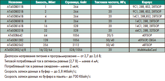
Atmel produces two families of SPI ROMs: the AT25 series based on EEPROM technology and the AT45 series based on Flash technology. In the AT25 series there are representatives based on Flash technology - these are AT25F512 / 1024 microcircuits. Flash chips of the AT25 series have a higher exchange rate, but fewer write cycles (10,000 times).
The main parameters of the AT25 series microcircuits are shown in Table 3.
Table 3
![]()
The history of the development of the AT45 family of microcircuits, which is based on the patented DataFlash ® architecture, which is the property of Atmel, is the most interesting. This family has already gone through several generations in its development. Chips of the first generation AT45D011 - AT45D161 were manufactured using 0.35 micron technology and had a supply voltage of 5 V (these microcircuits are no longer produced at present). Three digits in the name of the microcircuit mean the following: the first two - the capacity of the microcircuit in megabits, the third - the number of I / O ports. The die sizes were large enough that they were packaged in SOIC28 packages with most of the pins left unconnected. Thus, a microcircuit of any capacity could be installed in the same place. Soon Atmel mastered the production of microcircuits with a low voltage supply AT45DB011 - AT45DB321. The latest chip was released in the TSSOP32 package. After the transition to 0.25 micron technology, the die area has been significantly reduced, and now microcircuits with a capacity of 1, 2 and 4 Mbit are produced even in SOIC8 packages.
Although the SPI communication speed increased to 20 MHz with the transition to 0.25 micron technology, this was not enough for high-capacity chips. To eliminate the "bottleneck", chips with a capacity of 64 Mbit and higher began to be equipped with an additional 8-bit interface. Thus, the AT45DB642 chip can be accessed simultaneously via two ports, and the clock frequency for serial access is 20 MHz, for parallel access - 5 MHz.
The new DataFlash ® AT45DB1282 and AT45DB2562 chips, with capacities of 128 and 256 Mbit, respectively, are manufactured using 0.18 micron technology. This technology made it possible to increase the exchange rate to 50 MHz via the SPI interface and up to 40 MHz via the byte interface. If SOIC packages were considered standard packages for AT45 microcircuits of previous generations, then TSOP packages became standard for new high-capacity microcircuits.
Microcircuits are produced in cases different size(TSOP32, TSOP40 and TSOP48), however they are PCB compatible. If you look at the pinout of the microcircuits in the above packages, you can see that in the TSOP40 package, eight extreme pins (four from each edge) are not used. A similar situation is observed for the TSOP48 package, only the number of free pins here is sixteen. Thus, if the TSOP48 package is divorced on the printed circuit board, a microcircuit with a capacity of 64, 128 or 256 Mbit can be installed on this board.
The line of AT45 microcircuits currently produced has a capacity range from 1 Mbps to 256 Mbps. Chips with a capacity of 512 and 1024 Mbit are in the process of preparation for industrial production using 0.13 micron technology. In addition to the actual memory chips with SPI interface, Atmel also offers MMC (MultiMediaCard) format modules with a capacity of 2, 4 and 8 MB with a 7-pin connector and the corresponding interface.
Using the SPI interface allows the designer to move to higher capacity chips with minimal effort. As a rule, for this it is enough to change two constants in the program for working with the SPI ROM - the page size and the number of pages in this chip.

Unlike high-capacity Flash memory chips from other manufacturers, Atmel chips do not contain defective bits in the memory array, and there is no need for a data recording quality control procedure. AT45 ICs have 5V tolerant I/O, allowing direct connection to 5V microcontrollers.
The main parameters of the AT45 series microcircuits are given in Table. four.
Table 4
The article concludes with an example of the AT45 series memory function. An AVR microcontroller is used as a control processor. The program is written in C language for ImageCraft Company compiler. A 30-day demo version of this compiler can be found on the Atmel website at http://atmel.argussoft.ru/soft.htm. The file size is 3.9 MB. The included file at45.h is located at http://atmel.argussoft.ru/as-mega.htm.
One of the largest manufacturers of semiconductor electronic circuits is . Atmel's microcontrollers, non-volatile memory modules, complex logic integrated circuits, and semiconductor components for mixed signal processing can be found in the design of a huge number of electronics and other modern technology.Atmel product marking features
A unified labeling standard has been developed for the entire range of products manufactured by the company, which takes into account the diversity technical parameters one or another group of microcircuits.All chips manufactured by Atmel are labeled as AT XXXXX - X X X X (the X symbol here denotes alphabetic or numeric characters). Considering them in order, we get:
- AT - the designation of all microcircuits produced by the company;
- XXXXX - designate a group, type, manufacturing technology;
- X - indicates the speed of the device;
- X - a type of circuit body;
- X - operating temperature range;
- X - execution options.
- the group to which the circuit belongs (various types of memory, logic circuits, microcontrollers);
- types of memory (microprocessors, permanent and sequential memory, programmable and reprogrammable);
- the technology used to make the circuit;
Consider this example of labeling:ATMEGA165PV-8AU:

- after the first two letters, which indicate the manufacturer, follows the marking of the family to which this microcontroller belongs - MEGA;
- the numbers 16 correspond to the amount of flash memory built into the chip, expressed in kb;
- the number 5 indicates the version of the controller;
- letter P - picoPower manufacturing technology, which provides economical current consumption in mode up to 100 nA for Power down mode;
- V - corresponds to the operating voltage range from 1.8 to 5.5 volts;
- the number 8 indicates the maximum operating frequency of the microcircuit;
- the letter designation A corresponds to the TQFP case;
- U stands for chip operating temperature range from -40°C to +85°C and the need to use lead-free solder when working on the circuit.
"Directory"- information on various electronic components: transistors, microchips, transformers, capacitors, LEDs etc. The information contains everything necessary for the selection of components and carrying out engineering calculations, parameters, as well as the pinout of cases, typical wiring diagrams and recommendations for use radio elements.
Atmel® DataFlash® memory chips are ideal for a variety of technical applications, no matter what type of data you need to store. Since DataFlash functions like a high capacity serial EEPROM (Electrically Erasable Programmable Read-Only Memory), it can be used in many technical applications instead of it, which can significantly reduce the price. finished product. In this article, the AT45DBxx1D series microcircuits will be considered.
general description
The AT45DBxx1D series is ideal for use in a wide variety of technical applications where digitized data, speech, images or actual program code must be stored. All AT45DBxx1D series memory chips support the RapidS™ serial interface required for applications that require the device to operate at high data rates. The RapidS™ interface is SPI (Serial Peripheral Interface) compatible for clock speeds up to 66MHz. The entire memory of each of the representatives of this series is organized as a set of pages of a certain size. The number of pages and their size are determined depending on the specific chip model. In addition to the main memory, microcircuits of this series have one or two additional buffers of static RAM (see Table 1), which allow obtaining data during reprogramming ("flashing") of the main memory, as well as recording a continuous data stream. In this case, all reprogramming / erasing operations are self-synchronized. EEPROM emulation can be easily done with a stand-alone 3-step read/change/write procedure. Unlike regular Flash memory, which is random accessed with shared address buses and a parallel interface, DataFlash® chips use a RapidS™ interface for serial data access. Such a simple data access scheme significantly reduces the number of active pins of the microcircuit, which makes it possible to reduce the weight and dimensions of the device in which it is used, as well as increase its reliability and minimize switching noise. As such, the AT45DBxx1D series is optimized for use in a variety of commercial and industrial applications that require compactness, low voltage, and low power consumption. To simplify the "flashing" procedure for the AT45DBxx1D series microcircuit, a unipolar power supply with a voltage of 2.5 ... 3.6 V (or 2.7 ... 3.6 V) is required, depending on the type. Each chip in this series is controlled via a CS (Chip Select) crystal selection pin, and data is accessed via a 3-wire interface that includes a SI (Serial Input) serial input, a serial output (Serial Output) and clock synchronization (Serial Clock). ). Main distinctive features and characteristics of AT45DBxx1D series microcircuits are presented in Table. 1. Pinout of conclusions and appearance chips of the AT45DBxx1D series in various packages is shown in fig. one.
Rice. Fig. 1. Pinout and appearance of AT45DBxx1D series microcircuits in various packages: a - MLF8, b - SOIC8, c - TSOP28
Table 1. Main distinguishing features and characteristics of AT45DBxx1D series chips
|
Name |
Capacity,bit |
upit, B |
Interface |
RAM buffer, bytes |
Numberconclusions |
Type of shell |
The sizepages,byte |
Numberpages |
The sizeblock,kb |
The sizesectors,kb |
|
MLF8, TSOP28, SOIC8 |
||||||||||
Main Features of AT45DBxx1D Series Chips
Here are the main features of AT45DBxx1D series Flash memory chips:
Power supply from a unipolar source with a voltage of 2.5 ... 3.6 V or 2.7 ... 3.6 V;
RapidS™ interface (clock up to 66 MHz) SPI compatible;
User-configurable memory page size (see Table 1);
Intelligent programming function;
Flexible Data Wipe Options:
- the possibility of page / block / sector-by-sector erasure (see Table 1);
- complete erasure;
Additional static RAM buffers;
Ability to read a continuous stream of data (ideal for applications that use shadow RAM);
Low Power Consumption:
- 7 mA - in active mode;
- 25 µA - in standby mode;
- 5 µA (9 µA for AT45DB161D type chip) - offline;
Hardware and software protection functions;
Sector lock to protect program code or stored data;
Private access to data using a secret 128-byte register:
- 64-byte user-programmable space;
- 64-byte unique device identifier;
Compliance with JEDEC (Joint Electronic Device Engineering Council) standards;
Data storage period - 20 years;
The minimum number of "flashing" / erasing cycles per page is 100,000;
Work in the industrial temperature range (-40...+85°С);
Environmentally friendly body type.
Table 2 describes the pin functionality of the AT45DBxx1D series.
Table 2. Functional purpose pinouts of AT45DBxx1D series chips
|
Designation |
Functional purpose |
Activelevel |
Type ofsignal(input/exit) |
|
Crystal selection. Setting the active level on this pin allows access to the chip. In the case when there is no active level on this pin, the microcircuit operates in standby mode and a high resistance is set on the SO output pin. However, it cannot receive data on the SI input pin. Turning on the microcircuit is carried out by changing the signal level from high to low at the CS pin, and turning it off - by changing the level from low to high. Upon completion of internal self-synchronizing operations (such as a data write or an erase cycle), the chip enters standby mode only after they are completely completed. |
|||
|
Clock frequency of the serial interface. This pin is used to synchronize the operation of the chip and control the flow of data through this interface. The command, address, and input data on the SI pin are always clocked on the rising edge of SCK, while the output data on the SO pin is always clocked on the falling edge. |
|||
|
Serial interface input. This pin is used to input (using serial shift) all data stored in the chip, including commands and address sequences. Data on the SI pin is always clocked on the rising edge of SCK. |
|||
|
Serial interface output. This pin is used to output (using a serial shift) the data stored in the chip. The data on the SO pin is always clocked on the falling edge of SCK. |
|||
|
Write protection. When this pin is active, all memory sectors marked as protected in the Sector Protection Register will be unavailable for write or erase operations, regardless of whether the Enable Sector Protection command has been issued. or not. The WP output functions independently of the software-controlled protection method. Once the WP pin is driven low, the contents of the sector protection register cannot be changed. If the chip receives a write or erase command while the WP pin is active, it will ignore the command and return to idle mode (as soon as the CS pin becomes inactive). In this case, the microcircuit will only recognize commands to enable sector protection and sector lockdown (Sector Lockdown). The WP pin has a high resistance, so if hardware overwrite/erase protection control is not used, this pin can be left unconnected. It is recommended that WP be connected to VCC |
|||
|
Reset. A low level on this pin interrupts the current operation and puts the chip into standby mode. At the same time, it will be in reset mode as long as a low signal level is present at this pin. When the RESET pin is set high, the chip returns back to normal operation. The chip has an internal reset circuit (at power-up), so there is no restriction on resetting during the power-up procedure. If for some reason this pin is not used, it is recommended to keep the signal high on it. |
|||
|
RDY/BUSY (AT45DB161D, AT45DB321D only) |
Ready/Busy. This pin is driven low each time the chip performs a self-synchronizing operation (write/erase, compare, transfer data between buffer and page). The "busy" status indicates that access to the memory and one of the buffers is closed, while read / write operations from / to other buffers remain possible |
||
|
Source of power. The VCC pin is used to supply power from the source to the chip. It is strongly recommended to use only voltages specified by the manufacturer, as otherwise it may lead to malfunctions and memory errors. |
Source |
||
|
Earth."Ground" in relation to the power source. This pin must be connected to system ground. |
Functional diagram
The general functional diagram of the AT45DBxx1D series microcircuits (using the AT45DB041D as an example) is shown in fig. 2. The main blocks here are the Flash Memory Array, which stores the recorded data, the static RAM buffer (Buffer), which allows you to receive data when the microcircuit is "flashed", and also used as an independent address space for reading / writing incoming data and their further transfer to the main memory of the MSP (with subsequent erasure or without it), and the input / output interface (I / O Interface), through which control and access to the processed data is carried out.

Rice. 2. Functional diagram of the AT45DB041D chip
To provide optimally flexible data access, the memory matrix of the AT45DBxx1D series is divided into three types of segments: sectors, blocks, and pages. The number and size of sectors, blocks and pages depends on the specific type of microcircuit (see Table 1). At the same time, work is available in two addressing modes (selection of the mode by the appropriate command): binary (in which a space of a multiple of a power of 2 is addressed) and standard DataFlash® (when more memory is available, which provides additional data flow control). All software operations are performed at the "page" level, and only an erase operation can be performed on a page, sector, block, or directly on all available memory.
The operation of the microcircuit is controlled by commands coming from the host machine. Each instruction is clocked on the falling edge of the CS pulse and begins with an 8-bit opcode followed by the destination address (static RAM buffer or main memory matrix). When transmitting all address and data commands, the most significant bit is transmitted first.
In addition to standard read/write/erase operations, the family of microcircuits under consideration supports software and hardware methods for protecting against errors and incorrect data access. The software method is based on commands from the host machine that turn protection options on or off, while the hardware method works on a signal on the WP pin. The selection of memory areas to be protected and their current status is determined through the sector protection register and the status register (Status Register).
Limit and typical electrical characteristics on a permanent basis and alternating current AT45DBxx1D series chips are shown in Table. 3-5.
Table 3. Limiting electrical characteristics of AT45DBxx1D series microcircuits
Table 4. Typical DC Electrical Specifications for AT45DBxx1D Series Chips
|
Designation |
Parameter |
Terms |
Max. |
Unitsmeasurements |
||
|
Quiescent current |
||||||
|
Standby current |
CS*, RESET*, WP* = V IH , CMOS level on all inputs |
|||||
|
Operating current (read data mode) |
f = 20 MHz; I OUT = 0 mA; VCC=3.6V |
|||||
|
f = 33 MHz; I OUT = 0 mA; VCC=3.6V |
||||||
|
f = 50 MHz; I OUT = 0 mA; VCC=3.6V |
||||||
|
f = 66 MHz; I OUT = 0 mA; VCC=3.6V |
||||||
|
Operating current (Write/Erase mode) |
||||||
|
Input load current |
V IN = CMOS level |
|||||
|
Output leakage current |
V I / O = CMOS level |
|||||
|
Low input voltage |
||||||
|
High level input voltage |
||||||
|
Low output voltage |
IOL = 1.6 mA; VCC=2.7V |
|||||
|
High output voltage |
IOH = -100 uA |
* - low signal level is active.
Table 5. Typical AC Electrical Specifications for AT45DBxx1D Series (RapidS™/SPI Interface)
|
Designation |
Parameter |
Max. |
Unitsmeasurements |
|||
|
f SCK |
Clock frequency |
|||||
|
Clock rate for serial data reading |
||||||
|
Reduced clock speed for serial read data |
||||||
|
Page transfer time to static RAM buffer |
||||||
|
Page comparison time against static RAM buffer |
||||||
|
Page erasure and rewrite times |
256/264 bytes |
|||||
|
512/528 bytes |
||||||
|
Page rewrite time |
256/264 bytes |
|||||
|
512/528 bytes |
||||||
|
Page Erase Time |
256/264 bytes |
|||||
|
512/528 bytes |
||||||
|
Block Erase Time |
||||||
|
Sector Erase Time |
||||||
|
Reset pulse duration (RESET) |
||||||
|
Recovery time after reset |
||||||
Atmel Corporation is a world-famous manufacturer in the field of electronic components.
Product portfolio - logic microcircuits with a wide range of options, non-volatile memory modules, integrated circuits for RF and mixed signal processing. Today the company develops and manufactures electronic components used in industry, security systems, computer networks, and the automotive industry.
Atmel was founded in 1984. The company's headquarters is located in San Jose, California, USA. Since August 2006, Steven Laub has been President and CEO of the company. In total, the corporation employs about 5,100 employees. The founders of the company were the Greek brothers George and Gust Perlegos. Their family emigrated to California at a time when Silicon Valley was becoming a center of advanced information technology. After 8 years of experience at Intel, the eldest of the brothers decided to start his own business. He founded his own company and named it after the first letters of its intended specialization: Advanced Technology MEmory and Logic.
The start-up company was only 2 years old. Already in 1986, Atmel received a five-million dollar contract with General Instrument for the supply of a batch of electronic components.
In 1989, the company began to produce flash memory, in the early nineties - 1.8V microcircuits.
In 1995, the production of AVR microcontrollers was launched. Billion sales turnover Atmel reached already in 1996.
In 1998, Atmel bought shares in Telefunken Microelectronic, which allowed the corporation to enter the automotive electronics and communications market. In 2000, the production of image sensors and radio frequency information systems based on SiGe technology started.
In the history of the company there were not only successes, but also tangible declines. So, due to the incorrect definition of market needs, consumers of flash memory with enhanced characteristics were lost. Low-end models from Intel and AMD turned out to be more popular.
Products
Microcontrollers. The Atmel microcontroller line includes:
8 and 32 bit AVR microcontrollers. Today, 32-bit microcontrollers are used for those applications where an 8-bit microcircuit would be enough. But because the prices for these items are almost the same, developers using 32-bit devices can afford a performance headroom that is useful for future application upgrades.
Microcontrollers with ARM architecture. The ARM core basically contains the ideology of the RISC architecture: a limited set of instructions, active use registers, limited memory access. The 32-bit ARM instruction set includes instructions for accessing a hardware coprocessor, which allows developers to extend the capabilities of the underlying architecture by adding their own coprocessors if necessary.
- MCU Wireless Atmel microcontrollers focused on facilities wireless communication via ZigBee® and IPv6/6LoWPAN protocols.
- 8051 microcontrollers with 2 UART interfaces, watchdog timer, power failure detection circuit, PCA, SPI and in-circuit debugger, ideal for controlling I/O, power, motors.
Touch controllers for the market of portable devices with low power consumption, which are produced for touch panels new generation. The devices use QTouch® proprietary capacitive technology.
Non-volatile memory chips. The product line includes microcircuits with various interfaces, architectures and organizations, including page-by-page (Flash) and byte-by-byte (EPROM) memory access. These trace elements are especially widely used in applications where it is necessary to reduce the cost of the final product.
Reconfigurable FPSLIC SoCs. The essence of the technology is to place the AVR core, FPGA block and static memory array on one chip. The main advantages are an increased degree of integration, low power consumption, high performance.
Perspectives Atmel
Today, Atmel firmly holds the leading position in the world ranking in the production of a wide range of microcontroller devices and memory chips. In 2011, the company announced Xmega microcontrollers with USB interface and LCD controller. They are supposed to be used in industrial automation devices, sports and gaming applications, complex medical equipment, and security systems.
The entire range of Atmel multi-purpose microcontrollers is constantly being improved, new crystals appear, microcircuit versions are updated, and the software to support development.