AVR training course. Using the TWI module. Working with DS1307. Cheap and cheerful. Ch3. Static electrical characteristics. Absolute maximum values.
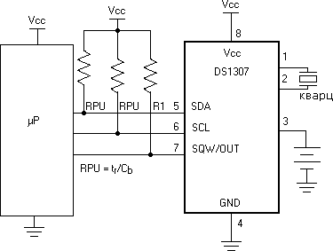
DS1307 8-pin DIP (300ms)
DS1307 8-Lead SOIC (150 mil)
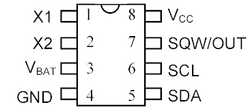
Pin assignment
V CC - primary power supply;
X1, X2 - connection of a 32.768 kHz quartz resonator;
V BAT - battery input +3 V;
GND is a common minus;
SDA - serial data;
SCL - serial sync pulses;
SQW / OUT - square-wave output signal.
Description
The DS1307 Serial Real Time Clock is a low power full BCD calendar clock with 56 bytes of NVRAM. Addresses and data are transferred serially over a two-wire, bidirectional bus. The calendar clock counts down the seconds, minutes, hours, day, date, month and year. The last date of the month is automatically adjusted for months with less than 31 days, including leap year adjustments. The watch operates in both 24-hour and 12-hour modes with AM / PM indicator. The DS1307 has a built-in power monitoring circuit that detects power interruptions and automatically switches to battery power.
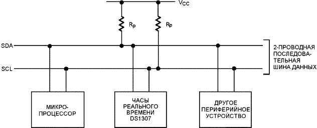
Typical connection scheme
Work
The DS1307 acts as a slave on the serial bus. Access to it is achieved by setting the START condition and transmitting an identification code to the device, followed by the register address. The following registers are accessed sequentially until the STOP condition is met.
If V CC falls below 1.25 * V BAT, DS1307 interrupts the access process and resets the address counter, during which time no external signals are received (to prevent writing erroneous data).
If V CC falls below V BAT, DS1307 switches to low current battery backup mode.
On power-up, DS1307 switches from battery to Vcc when Vcc exceeds V BAT + 0.2 V... Incoming signals are perceived when Vcc exceeds 1.25 * V BAT.
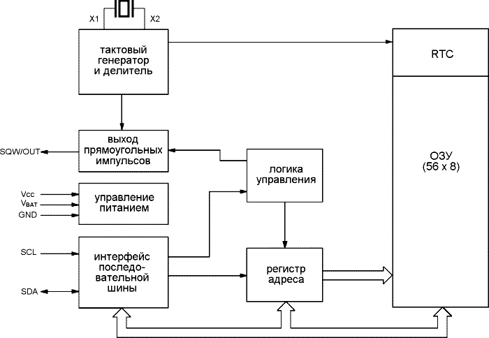
Block diagram on Rice. one shows the main elements of a serial RTC.
Rice. one. DS1307 block diagram
Pin Description
V CC, GND- these outputs are powered.
V CC is the +5 V input. When the supply voltage is higher 1.25 * V BAT, the device is fully accessible and you can read and write data. When a 3V battery is connected to the device, and V CC is lower than 1.25 * V BAT, reading and writing are prohibited, but the timing function continues to work. As soon as V CC falls below V BAT, the RAM and RTC are switched to battery-powered V BAT.
V BAT- input for any standard 3-volt lithium battery or other power source. For normal work The DS1307 requires a battery voltage in the range of 2.0 ... 3.5 V. A lithium battery with a capacity of 48 mAh or more will support the DS1307 for more than 10 years at a temperature of 25 ° C in the absence of power.
SCL(Serial Clock Input) - used to synchronize data over the serial interface.
SDA(Serial Data Input / Output - input / output of serial data) - input / output pin for two-wire serial interface... The SDA pin is open drain and requires an external pull-up resistor.
SQW / OUT(Square Wave / Output Driver) - when enabled, i.e. the SQWE bit is set to 1, the SQW / OUT pin outputs square-wave pulses at one of four frequencies (1 Hz, 4 kHz, 8 kHz, 32 kHz). The SQW / OUT pin is open drain and requires an external pull-up resistor. SQW / OUT will operate on both V CC and V BAT power.
X1, X2- leads for a standard quartz resonator with a frequency of 32.768 kHz. The internal clock is designed to work with a crystal resonator with an input capacitance of 12.5 pF.
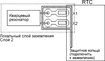
More detailed information the choice and location of the quartz resonator can be found in the application example № 58 "Crystal Considerations with Dallas Real-Time Clocks" (Application Note 58, "Crystal Considerations with Dallas Real-Time Clocks"). The DS1307 can also be clocked by an external 32.768 kHz clock. In this case, the X1 pin is connected to the signal of the external clock generator, and the X2 pin remains unconnected.
Clock accuracy
The accuracy of the watch depends on the accuracy of the quartz resonator and the accuracy of the match between capacitive load of the clock generator circuit and internal capacitance of a quartz resonator... An additional error will be introduced by the drift of the frequency of the quartz resonator, which occurs due to temperature differences. Interference and noise from external circuitry can lead to faster synchronization.
More detailed information see application example № 58 "Crystal Considerations with Dallas Real-Time Clocks" (Application Note 58, "Crystal Considerations with Dallas Real-Time Clocks"). For more information, see the application example. № 95 "Interfacing the DS1307 with a 8051-Compatible Microcontroller" (Application Note 95, "Interfacing the DS1307 with a 8051-Compatible Microcontroller").
RTC and memory card
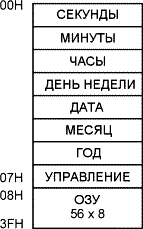
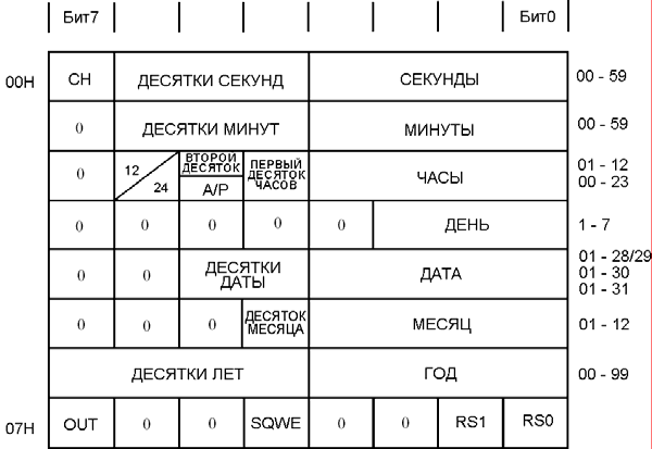
The address map for RTC and RAM registers is presented on Rice. 2. The RTC registers are located in address locations 00h to 07h. The RAM registers are located in the addresses from 08h to 3Fh. During multibyte access, when the address pointer reaches 3Fh (end of RAM space), it is moved to location 00h - the beginning of RTC space.
Rice. 2. DS1307 Address Map
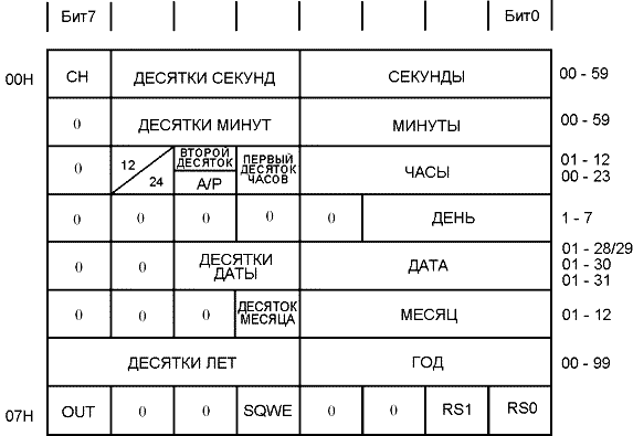
Clock and calendar
Information from the clock and calendar is obtained by reading the corresponding register bytes. The RTC registers are shown in Rice. 3... Time and calendar are set or initialized by writing the appropriate register bytes. The contents of the time and calendar registers are in BCD format. Bit 7 of register 0 is the clock halt (CH) bit. When this bit is set to 1, the clock generator switched off... When cleared to 0, the clock generator is on.
Note that the initial state of all registers is undefined at power up. Therefore, it is necessary to forcibly turn on the clock generator (bit CH = 0) during initial initialization.
DS1307 can operate in both 12-hour and 24-hour modes. Bit 6 of the clock register is responsible for selecting 12- or 24-hour mode. When it is set to 1, 12 hour mode is selected. In this mode, bit 5 is the AM / PM bit, with a logic high indicating PM. In 24-hour mode, bit 5 is the bit in the second ten hours (20-23 hours).
When the START condition appears on the two-wire bus, the current time is copied into the second set of registers. Time information is read from these auxiliary registers while the clock can continue to run. This eliminates the need to re-read the DS1307 registers if their contents are updated while reading.
Rice. 3. Chronometer registers DS1307
Control register
The control register is used to control the operation of the SQW / OUT pin.
BIT 7 BIT 6 BIT 5 BIT 4 BIT 3 BIT 2 BIT 1 BIT 0 OUT 0 0 SQWE 0 0 RS1 RS0 OUT(Output control) - This bit controls the logic level on the SQW / OUT pin when the square wave output is disabled. If SQWE = 0, then the logic level at the SQW / OUT pin is 1 if OUT = 1, and 0 if OUT = 0.
SQWE(Square Wave Enable) - When this bit is set to 1, square wave generation is enabled. Their frequency depends on the meaning of the RS0 and RS1 bits. (If the output frequency is set to 1Hz, the clock registers are updated on the falling edge of these pulses.)
Rs(Rate Select) - These bits control the frequency of the square wave when the SQWE bit is 1. V Table 1 the frequencies that can be selected using the RS bits are shown.
Table 1. SQW output frequency
RS1 RS0 Frequency 0 0 1 Hz 0 1 4.096 kHz 1 0 8.192 kHz 1 1 32.768 kHz Two-wire serial data bus
DS1307 supports I2C communication over a two-wire, bidirectional bus. The device that transmits data to the bus is the transmitter, and the device that receives the data is the receiver. The device that controls the transmission of data is called the master. The device controlled by the master is called the slave. The master generates serial clock (SCL), controls bus access, and generates START and STOP conditions. The DS1307 acts as a slave on the bus. A typical bus configuration using the I2C protocol is shown in Rice. 4.
Rice. 4. Typical 2-Wire Bus Configuration
On the Rice. 5, 6 and 7 The process of transferring data on a two-wire bus is shown in detail.
Basic principles of data transfer via the I2C bus:
1) Data transfer can only be initiated when the bus is free.
2) During transmission, the data on the SDA line can only change when the SCL line is low, otherwise the data change will be interpreted as a control signal.
Thus, the following bus states are possible:
- Bus not busy - the high level remains on the SDA and SCL lines.
- Start of data transfer (START condition) - change the state of the SDA line from high to low, while the SCL line is high.
- End of data transfer (STOP condition) - changing the state of the SDA line from low to high, while the SCL line is high.
- Correct data - the state of the SDA line represents correct data, if after the START condition the state of the SDA line does not change for high level clock signal. The data on the line should change during the period low level clock signal. There is one clock pulse per bit of data.
Each data transfer is initiated with a START condition and terminated with a STOP condition. The number of data bytes transferred between the START and STOP conditions is unlimited and is determined by the master. Information is transmitted byte-by-byte, and each byte is confirmed by the receiver with the ninth bit (confirmation bit - ACK). The 2-wire interface specification defines the normal mode (with clock frequency 100 kHz) and fast mode (400 kHz clock rate). DS1307 only operates in normal mode (100 kHz).
- Confirmation - each receiving device, when addressed, is obliged to generate an acknowledgment after receiving each byte. The master must generate an additional clock pulse, which is for the acknowledge bit.
The acknowledgment device should pull the SDA line low during the acknowledgment clock so that the SDA line remains stable low during the acknowledgment clock high period. Of course, tuning and retention times must be taken into account. The master should signal the slave the end of the data without generating an acknowledge bit on the last byte that was received from the slave. In this case, the slave must leave the data line high to allow the master to generate a STOP condition.
* - read / write bit or direction bit
Rice. 5. 2-wire serial data transmission
Two types of data transmission are possible depending on the state of the bit:
1) Data transmission from the master transmitter to the slave receiver.
The first byte transmitted by the master is the slave address. This is followed by a number of data bytes. The slave returns an acknowledgment bit after each received byte. Data is transmitted starting with the most significant bit (MSB).
2) Data is transmitted from the slave transmitter to the master receiver.
The first byte (slave address) is transmitted by the master. The slave returns an acknowledgment bit. This is followed by a number of data bytes transmitted by the slave. The master returns a confirmation bit after all received bytes except the last byte. A non-acknowledgment is returned at the end of the last byte received. The master generates all serial sync pulses as well as START and STOP conditions. The transfer ends with a STOP condition or a repeat of the START condition. Since the repetition of the START condition is also the start of the next serial transmission, the bus is not released. Data is transmitted starting with the most significant bit.
DS1307 can operate in the following two modes:
1) Slave receiver mode (DS1307 recording mode).
Serial data is received over SDA and synchronized over SCL. A confirmation bit is transmitted after each received byte. The START and STOP conditions are recognized as the beginning and end of a serial transmission. Address recognition is performed in hardware after receiving the slave address and direction bit (see chap. Rice. 6).
The address byte is the first byte received after the master has generated a start condition. It contains 7 bits of the DS1307 address, which is 1101000 , and the following direction bit (), which for writing is 0. After receiving and decoding the address byte, DS1307 issues an acknowledgment to the SDA line, after which the master sends the register address to the device. This will set the register pointer. The master then starts transmitting data bytes, each of which will be acknowledged by the DS1307. The master generates an end condition to finish writing data.
Rice. 6. Data Logging - Slave Receiver Mode
2) Slave Transmitter Mode (DS1307 Read Mode).
The first byte is received and processed in the same way as in slave receiver mode. However, in this mode, the direction bit will indicate that the transmission direction is inverted. The DS1307 transmits serial data over the SDA line while serial sync pulses are sent to the SCL line. START and STOP conditions are recognized at the beginning and at the end of a serial transmission (see chap. Rice. 7).
Address Byte - The first byte received after the start condition is generated by the master. The address byte consists of the 7-bit DS1307 address, which is 1101000 , and the next bit of the direction of transmission (), which for reading is 1. After receiving and decoding the address byte, the device issues an acknowledgment to the SDA line. The DS1307 then starts transmitting data starting at the specified address in the register pointer. If before the start of reading the register pointer is not written, then the first readable address is the address that was last saved in it. The DS1307 must accept a non-acknowledgment to end the read.
Rice. 7. Reading Data - Slave Transmitter Mode
Absolute maximum values *
Voltage at any terminal to ground: -0.5 V to +7.0 V.
Storage temperature: -55 ° C to +125 ° C.
Soldering temperature: 260 ° C for DIP at 10 seconds exposure.
For surface mount devices, see JPC / JEDEC standard J-STD-020A.
* These are limit values only, and operation of the device under these or any conditions more severe than those specified in the operating sections of this datasheet is not implied. Operation at absolute maximum values for a long period of time may affect the reliability of the device.
(Above working range *)
* Unless otherwise agreed
Static electrical characteristics
(Above working range *)
Parameter Designation Meaning Units
measurementsNote Minimum Typical Maximum Input Leakage Current (SCL) I LI 1 μA Leakage current input / output (SDA and SQW / OUT) I LO 1 μA Logic 0 output (IOL = 5 mA) V OL 0.4 V Active supply current I CCA 1.5 mA 7 Storage current I CCS 200 μA 1 Battery current (OSC on); SQW / OUT off I BAT1 300 500 on the 2 Battery current (OSC on); SQW / OUT on (32 kHz) I BAT2 480 800 on the Power failure voltage V PF 1.216 x V BAT 1.25 x V BAT 1.284 x V BAT V 8 * Unless otherwise agreed
Dynamic electrical characteristics
(Above working range *)
Parameter Designation Meaning Units
measurementsNote Minimum Typical Maximum SCL clock frequency f SCL 0 100 kHz Bus downtime between STOP and START conditions t BUF 4.7 μs Holding time (repetition) of the START condition t HD: STA 4.0 μs 3 SCL sync low period t LOW 4.7 μs SCL high period t HIGH 4.0 μs Setting time for repeated START condition t SU: STA 4.7 μs Data retention time t HD: DAT 0 μs 4, 5 Data setup time t SU: DAT 250 ns Rise time for SDA and SCL signals t R 1000 ns Fall time for SDA and SCL signals t F 300 ns Setting time for STOP condition t SU: STO 4.7 μs C B 400 pf 6 Capacitance I / O (T A = 25 ° C) C I / O 10 pf Capacitive loading determined by a quartz resonator (T A = 25 ° C) 12.5 pf * Unless otherwise agreed
Notes:
1.I CCS is indicated when V CC = 5.0V and SDA, SCL = 5.0V.
2.V CC = 0V, V BAT = 3V.
3. After this period, the first sync pulse is generated.
4. The device must internally provide a hold time of at least 300 ns for the SDA signal (given the V IHMIN parameter of the SCL signal) in order to overcome the undefined region of the SCL trailing edge.
5. Maximum t HD: DAT should only appear if the device does not stretch the t LOW period of the SCL signal.
6. C B - total capacitive impedance of the bus line in pF.
7. I CCA - SCL synchronization at maximum frequency (100 kHz).
8. V PF measured at V BAT = 3.0 V.
Rice. eight. Timing diagram


Hello everyone. To work with the watch, the TWI interface was considered, which we will refer to today. Well, let's start. This clock is TWI compatible, i.e. the principle of data exchange via the bus will be the same as we have considered.
The figure below shows the location of the conclusions, the description, and the very look of our clock, or as we will call them later. RTC (Real-time clock) - real time clock or time pulse generator. This "device" counts seconds, minutes, hours, day of the month, month, day of the week and year, together with leap years. The calendar is valid until 2100. I think that's enough for our age :). 
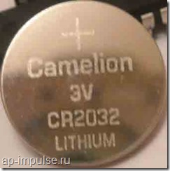
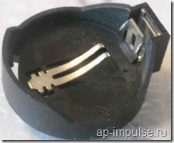
As you can see from the description, there is an input for emergency power supply from the battery, when the external power supply is disconnected. In this mode, the RTC supports only its main purpose - timing, without external requests. The battery supply voltage should be 2 - 3.5V. V technical description it is written that with a charge of more than 48 mA / h, at a temperature of 25 degrees Celsius, our circuit will last about 10 years. More than necessary. The picture below shows the CR2032 "tablet" and the mount that we will use.
Now let's go over the external power supply. The working voltage of the watch is 5V with a small range of 4.5 -5.5V. Battery voltage 3V (minimum 2, maximum 3.5V) RTC operation is divided into three voltage modes:
1. Vcc = 5V - reading, writing, counting;
2. Vcc = below 1.25 * Vbat, but above Vbat + 0.2V - only battery reading from external power supply.
3. Vcc below Vbat: RTC and RAM go to battery power. Consumption in active state 1.5 mA, from battery 500-800 nA.
Voltage for transmitting / receiving information:
Logic 0: -0.5V - + 0.8V
Logic 1: 2.2V - Vcc + 0.3V
As in previous posts, let's try to run it in Proteus. Let's debug the code. And we will transfer everything to iron. Below is the connection diagram.

Where SQW / OUT is a clock output that can be programmed to output frequencies of 1Hz, 4.096Hz, 8.192Hz and 32.768Hz. Those. can be used to interrupt the controller externally at 1 s intervals. A very useful feature. But it won't be useful to us. By the way, it is also with an open collector, so a pull-up resistor is needed. The nominal is 4.7 kOhm.
Conclusions X1 and X2 - we connect a quartz resonator with a frequency of 32.768 kHz to them. Alternatively, you can use an external clock generator with the same frequency. But at the same time, the X1 pin is connected to the signal, and X2 remains unconnected (hang in the air.).
Well, the conclusions of SDA and SCL, which we met in the last article.
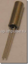
Let's dwell a little on the resonator (figure below). Which can be called the heart of the watch, and on which the accuracy of the movement depends. The quality of the resonator itself lies on the conscience of the manufacturer, but on our part, we can reduce the error introduced by external factors, if we adhere to the following recommendations for the placement of the resonator:
2. The width of the path should also be made as small as possible to reduce the likelihood of receiving interference from other sources.
3. A protective ring should be placed around the crystal to help isolate the crystal from noise.
4. Place the conductors in the ring and connect to earth.
5. Solder the resonator to the ground. If the land is divorced correctly and there is confidence.
The figure below shows the contour and the place of the fast ice to the ground.

We figured out how to connect. Go ahead and figure out how to work with it. RTC is programmable and has 8 bytes of special registers for its configuration and non-volatile static memory of 56 bytes. To exchange information, a 2-wire data bus is required, i.e. serial data bus - which we covered in the last article. So for work, let's go over the datasheet. What we need:
Register table. Figure below. The first eight registers are for displaying and programming our watch. When addressing 00H to the 7th bit (CH) and setting it to 0, we start the clock. I would like to note that the configuration of the registers can be any, therefore, at the first start, you need to configure it to suit your requirements. The remaining seven bits are ones and tens of seconds.

01H - Minutes.
02H - Clock to be adjusted:
- Bit 6 - for 1 output 12 hour format, 0 - 24.
- Bit 5 - at 1 (at 12 hour format) PM, 0-AM
- Bit 5 - (with 24 hour format) this is the output of the second ten hours (20-23 hours.)
- Bit4 - the first ten hours, the rest of the bits are hours.
03H - day of the week;
04H - date;
05H - month of the year
06H - year.
Well, the last register is 07H. This register is a control register, where OUT is responsible for controlling the SQW / OUT pin. Below is a table of output enable.
OUT |
SQWE |
SQW / OUT |
1 |
0 |
1 |
0 |
0 |
0 |
SQWE - when this bit is set to 1, pulses are output at the output with a specified frequency, which is set by the RS1 and RS0 bits.
This conclusion will not be useful to us in the project. Although for him, I spread a path on the board. As experiments, it may be somewhere in the future and applicable, because here you can make an interrupt of 1 s.
Now that we have all the necessary information, we will write functions for working with the clock. And also we will launch the project in Proteus ... Which will look like this:

Please note that the resonator in Proteus does not need to be connected to the clock (circled in red).
The figure shows the clock terminal, which displays the time, which in turn is tied to the system time. I2C protocol debugger terminal or TWI , which displays the time of sending and receiving the signal, where D0 is the transmitted command, D1 is the receiving. Below I will display screenshots of the terminal with the result of the program.
Program ... Having considered the basic clock settings, we will write an initialization function.
/ * The initialization function includes setting the baud rate according to the formula (in the previous article), setting the limit and enabling the TWI module * /
void init_DS1307 (void)
{
TWBR = 2; / * At a frequency of 1 MHz * /
TWSR = (0<< TWPS1)|(0 << TWPS0); / * Pre-divisor by 64 * /
TWCR | = (1<< TWEN); / * Enable TWI module * /
}
void write_DS1307 (uint8_t reg, uint8_t time)/ * we pass two parameters: the address of the register to which we will address and the transmitted information * /
{
/ * We form the START state by setting the bits of the control register * /
TWCR = (1<
/ * Allow the TWEN module to work; Form the state start TWSTA; Clear TWINT flag * /
/ * We are waiting for the end of the formation of the start condition, i.e. until the flag is set, status code = 08 * /
while (! (TWCR & (1<
/ * Next, we transfer the address packet (device address). The contents of the package are loaded into the TWDR register * /
TWDR = 0xd0; / * 0b1101000 + 0 - address + write bit * /
/ * Reset the flag for transferring information * /
TWCR = (1<
/ * Waiting for the flag to be set * /
while (! (TWCR & (1<
/ * pass the register to which we will refer * /
TWDR = reg;
TWCR = (1<
while (! (TWCR & (1<
/ * Pass information to be written to the register byte * /
TWDR = time;
TWCR = (1<
while (! (TWCR & (1<
/ * form the STOP state * /
TWCR = (1<
}
In this function, we transferred three bytes, the device address, the register address and a byte of information to write to this register and formed the STOP state.
The last read function remains. Below is the reading format.
This function transfers the device address byte + write bit, the register address byte for setting the pointer to it, the POVSTAR condition is fulfilled, the device address byte + read bit is transferred, the register whose address we transferred earlier is transferred.
If we refer to the clock in the read format, then when the clock is accessed again, the pointer is shifted one byte down, including 56 bytes of RAM, from 00H to 3FH. Upon reaching the last address, the pointer jumps to address 00.
/ * Function for reading data from DS1307 * /
uint8_t read_DS1307 (uint8_t reg)/ * Pass the register address * /
{
uint8_t time;
/ * form the START state * /
TWCR = (1<
while (! (TWCR & (1<
TWDR = 0xd0; / * Pass address + write bit * /
TWCR = (1<
while (! (TWCR & (1<
TWDR = reg; / * Register address * /
TWCR = (1<
while (! (TWCR & (1<
/ * form the POSTAR state * /
TWCR = (1<
while (! (TWCR & (1<
TWDR = 0xd1; / * Pass address + read bit * /
TWCR = (1<
while (! (TWCR & (1<
/ * read data * /
TWCR = (1<
while (! (TWCR & (1<
/ * form the STOP state * /
TWCR = (1<
return time;
}
So above we have written three functions that we need to work with the clock. Using these functions, we will launch the program in Proteus. Let's display, for example, the date.
#include
#include
uint8_t time;
void init_DS1307 (void);
uint8_t read_DS1307 (uint8_t reg);
void write_DS1307 (uint8_t reg, uint8_t time);
int main (void)
{
DDRC = 0x00; / * Set port as input * /
PORTC = 0xFF; / * Pull up resistance * /
init_DS1307;
while (1)
{
_delay_ms (50);
read_DS1307 (0 × 04); / * Read date register * /
}
}
Below is the result of executing the program reading the date.

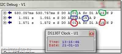
In the debugger window I2C
you can see that first the address of the register is sent to the RTC (green circle), in this case 04, which is responsible for the date of the month, and then the clock sends the answer 21 (red circle).
When we start the clock in the hardware, we will need to enter the present time. Below is an example of a program for changing the minutes.
while (1)
{
_delay_ms (500);
read_DS1307 (0x01); / * Read the minute * /
_delay_ms (500);
write_DS1307 (0x01,15); / * Write down the required minute * /
_delay_ms (500);
read_DS1307 (0x01); / * Read the minute * /
}
The figure shows that first there is a call to register 01, minute 23 is read. Next, we use the write function, and enter the value 15. At the next read function, we have the value 15 on the clock display.
Well, the last example of the program is the output of the values of all registers.
while (1)
{
delay_ms (500);
read_DS1307 (0x00);
_delay_ms (500);
read_DS1307 (0x01);
_delay_ms (500);
read_DS1307 (0 × 02);
_delay_ms (500);
read_DS1307 (0 × 03);
_delay_ms (500);
read_DS1307 (0 × 04);
_delay_ms (500);
read_DS1307 (0 × 05);
_delay_ms (500);
read_DS1307 (0x06);
_delay_ms (500);
}
The figure below shows that the data of 7 registers was displayed.
The source with the project is attached:
(Downloaded: 341 people)
That's all. Let's connect the clock in hardware, display the time on the indicator and get acquainted with the binary-decimal format for working with the clock. Goodbye to everyone.
DS1307 Real Time Clock Module
Tiny RTC I2C module 24C32 memory DS1307 clock
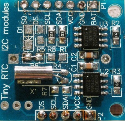
A small module that performs the functions of a real time clock. It is based on the DS1307ZN + microcircuit. Continuous timing is due to autonomous power supply from the battery installed in the module. The module also contains 32 Kbyte EEPROM memory, which retains information when all types of power are turned off. Memory and clock are linked by a common I2C interface bus. I2C bus signals are output to the module contacts. When an external power supply is connected, the battery is recharged through a primitive recharging circuit. There is space on the board for mounting a DS18B20 digital temperature sensor. It is not included in the package.
The use of this device occurs when measuring time intervals of more than a week with devices based on a microcontroller. It is unjustified and often impossible to use the MK's own resources for this purpose. It is expensive to provide uninterrupted power supply for a long time; it is impossible to install a battery to power the MK because of the significant current consumption. This is where the DS1307 real-time clock module comes to the rescue.
Also, the DS1307 real-time clock module, thanks to its own memory, allows you to record data from events that occur several times a day, for example, temperature measurements. The event log is then read from the module memory. These capabilities allow the module to be used as part of an autonomous automatic weather station or for climate research in hard-to-reach places: caves, rock tops. It becomes possible to register tenso parameters of architectural structures, for example, bridge supports and others. When equipping the device with radio communication, it is enough to install it in the surveyed area.
Specifications
Supply voltage 5 V
Dimensions 27 x 28 x 8.4mm
Electrical diagram
The device communicates with the device electronics using SCL and SDA signals. IC2 is a real time clock. Capacitors C1 and C2 reduce noise on the VCC power line. Resistors R2 and R3 ensure the SCL and SDA signals are at the correct level. IC2's pin 7 outputs a 1 Hz square wave signal SQ. It is used to test the functionality of MS IC2. Components R4, R5, R6, VD1 provide recharging of the BAT1 battery. For data storage, the DS1307 real-time clock module contains IC1, a non-volatile memory. US1 - temperature sensor. Signals of the module and power lines are routed to connectors JP1 and P1.
Data bus
I2C is a standard serial interface with two signal lines SCL, SDA and a common wire. The interface lines form a bus. Several microcircuits can be connected to the I2C interface lines, not only the microcircuits of the module. To identify the microcircuit on the bus, namely, writing data to the required MS and determining from which MS the data is coming. Each microcircuit has a unique address for the laid bus. DS1307 has Address 0x68. It is recorded at the factory. The memory chip has an address of 0x50. The Arduino software includes a software library that provides I2C support.
Real time clock microcircuit
DS1307 has low power consumption, communicates with other devices via I2C interface, and contains 56 bytes of memory. Contains a clock and a calendar until 2100. The real-time clock microcircuit provides other devices with information about the present moment: seconds, minutes, hours, day of the week, date. The number of days in each month is counted automatically. There is a compensation function for leap years. There is a flag to define whether the clock is running in 24-hour mode or 12-hour mode. To operate in 12-hour mode, the microcircuit has a bit from which data is read for transmission about a period of time: before or after lunch.
Long-term memory chip

Illustration of the DS1307 real-time clock module from the battery side with the U1 temperature sensor installed.
Battery
The holder on the back of the board holds a CR2032 lithium disk battery. It is available from many manufacturers, such as one manufactured by GP, which provides 3.6 V and 210 mAh discharge current. The battery is recharged when the power is turned on; this is the mode of operation of a lithium battery that we encounter on the motherboard of a computer.
Recharging the battery
Software
For the module to work as part of the Arduino, an outdated library from the Adafruit website called RTCLib is quite suitable. The sketch is called DS1307.pde. There is an updated version. Download the archive, unpack it, rename and copy the library to your Arduino library directory.
Connecting to Arduino Mega
To do this, use sketches.
SetRTC sets the time in hours according to the time shown in the sketch.
GetRTC displays the time.
Both sketches require the Wire library and define an I2C address. To set the clock address on the I2C bus, use this I2C scanner.
Arduino Mega connection.

Connect SCL and SDA to the corresponding pins 21 and 20 on the Arduino Mega 2560. Connect the power.
Arduino Uno connection
Set time in SetRTC sketch and upload to Arduino. Then press the reset button to set the clock. Now download the GetRTC sketch. Open the serial monitor and watch. There is a special time library. It has many different functions that can be useful depending on the situation. To set the time using the library you need to download. When using a sketch, you can synchronize the real-time clock with the clock of your personal computer.
 Vbat- battery input for any standard 3 Volt lithium cell or other power source. For normal operation, the battery voltage must be maintained between 2.5 and 3.5 V. The level at which access to the real time clock and user RAM is denied is internally set to 1.25 x Vbat. A lithium battery with a capacity of 35 mAh or more is sufficient to power the DS1307 for more than 10 years without power.
SCL(Serial Clock Input) - SCL is used to synchronize data transmission over the serial interface.
SDA(Serial Data I / O) - SDA - data I / O for 2-wire serial interface. This is an open drain output that requires an external pull-up resistor.
SQW / OUT(Square Wave / Output Driver) - When the SQWE bit is set to 1, the SQW / OUT outputs a square wave of one of four frequencies: 1 Hz, 4 kHz, 8 kHz, 32 kHz. The SQW / OUT pin is open drain and requires an external pull-up resistor.
X1, X2- pins for connecting a standard crystal of quartz 32.768 kHz. The internal circuit of the generator is designed to operate with a crystal having a nominal capacitance (CL) of 12.5 pF.
GND- Land.
VCC- power supply 5 volts.
DS1307 works as a slave on the serial bus. To access it, you need to set the state START and transmit the device identification code followed by the register address. Subsequent registers can be accessed sequentially until the state is set. STOP... When VCC falls below 1.25 x Vbat, the device stops communicating and resets the address counter. During this time, it will not respond to input signals to prevent the recording of erroneous information. When VCC drops below Vbat, the device switches to low power storage mode. When powered on, the unit switches power from battery to VCC when the supply voltage exceeds Vbat + 0.2V, and reacts to input signals when VCC will become more than 1.25 x Vbat. When the power is within normal limits, the device is fully accessible and data can be written and read. When a 3V battery is connected to the device and VCC is lower than 1.25 x Vbat, reading and writing is prohibited. However, the countdown works. When VCC drops below Vbat, the RAM and timing power supply switches to an external 3 V battery.
Time and date information is obtained by reading the corresponding registers. The clock registers are shown in the table below. Time and calendar are set or initialized by writing bytes to the appropriate registers. The contents of the time and calendar registers are stored in BCD (BCD) format, therefore, before displaying information on the LCD display or seven-segment indicator, it is necessary to convert the binary-decimal code to a binary or ANSII code.
Bit 7 of register 0 is the Clock Halt bit. When this bit is set to 1, the generator is stopped. When reset to zero, the generator is running and the clock is counting the time.
DS1307 can operate in 12-hour or 24-hour mode. Bit 6 of the clock register specifies one of these modes. When it is 1, the 12 hour mode is set. In 12 o'clock mode, bit 5 high indicates afternoon time. In 24-hour mode, bit 5 is the second bit of 10 hours (20-23 hours).
The DS1307 control register is designed to control the operation of the output SQW / OUT... Bit OUT- output control. This bit controls the output level on the pin. SQW / OUT when the generation of the meander is disabled. If SQWE = 0, the logic level on the pin SQW / OUT equals 1 if OUT= 1, and 0 - if OUT = 0. SQWE- Resolution of the meander. When this bit is set to 1, square wave generation is enabled. The square wave frequency depends on the values of the RS0 and RS1 bits. These bits control the frequency of the square wave when it is enabled. The table below shows the frequencies that can be specified by the RS bits.

DS1307 supports bi-directional 2-wire bus and communication protocol. The device that sends data to the bus is called a transmitter, and the device that receives the data is called a receiver. The device that controls the transmission is called the master. Devices controlled by the master are slaves. The bus must be controlled by a master that generates sequential clocks (SCL), controls access to the bus, and generates START and STOP states. DS1307 acts as a slave on a 2-wire bus.
To work with DS1307, it is necessary to organize the read function from the microcircuit and the write function.
1. DS1307 recording mode... Serial data and clocks are received via SDA and SCL. After the transmission of each byte, a confirmation bit is transmitted. ASK... States START and STOP are recognized as the beginning and end of the serial transmission. Address recognition is performed in hardware after receiving the slave address and direction bit. The address byte contains the 7-bit DS1307 address, equal to 1101000, followed by the direction bit (R / W), which when written is 0. After receiving and decrypting the address byte, the DS1307 issues an acknowledgment ASK on the SDA line. After the DS1307 confirms the slave address and write bit, the master transmits the DS1307 register address. This will set the register pointer in DS1307. The master will then start transmitting data bytes to the DS1307, which will acknowledge each byte received. At the end of the recording, the presenter will form a state STOP.
2. Reading mode from DS1307... The first byte is received and processed as in slave receiver mode. However, in this mode, the direction bit will indicate that the transmission direction has been reversed. Serial data is sent over SDA from the DS1307, while serial clocks are sent over SCL from the DS1307. States START and STOP are recognized as the beginning and end of the serial transmission. Address byte - the first byte received after the master has generated a state START... The address byte contains the 7-bit DS1307 address, equal to 1101000, followed by the direction bit (R / W), which when read is 1. After receiving and decrypting the address byte, the DS1307 issues an acknowledgment ASK on the SDA line. The DS1307 then starts transmitting data starting at the register address pointed to by the register pointer. If the register pointer is not written before initiating the read mode, then the first address that is read is the last address remaining in the register pointer. DS1307 should get unacknowledged NOASK to finish reading.
Let's consider the features of working with DS1307 using a simple clock as an example, which will show hours, minutes and seconds. The data will be displayed on a 16x2 LCD display. Two buttons "Hours +" and "Minutes +" will allow you to set the desired time. The Atmega 8 microcontroller is clocked by an internal 1 MHz oscillator, so don't forget to change the fuses. Below is a connection diagram.

The control program includes a set of functions for working with the TWI bus, DS1307 clock, LCD display.
I2CInit - bus initialization;
I2CStart - transmission of the START condition;
I2CStop - transmission of the STOP condition;
I2CWriteByte - data writing;
I2CReadByte - reading data;
DS1307Read - function for reading data from DS1307;
DS1307Write - Function of writing data to DS1307;
lcd_com - sending a command to the LCD;
lcd_data - data transfer to LCD;
lcd_string - function for displaying a string in the LCD;
lcd_num_to_str - function for outputting a character of int type;
lcd_init - LCD initialization.
Below is the program code:
#include #include // Function initialization of the TWI bus void I2CInit (void) (// setting the TWI module TWBR = 2; TWSR = (1<< TWPS1)|(1 << TWPS0); // Предделитель на 64
TWCR |= (1 << TWEN); // Включение модуля TWI
}
void I2CStart(void)
{
// Передача условия СТАРТ
TWCR = (1 << TWINT)|(1 << TWEN)|(1 << TWSTA);
// Ожидание установки флага TWINT
while(!(TWCR & (1 << TWINT)));
}
void I2CStop(void)
{
TWCR = (1 << TWINT)|(1 << TWEN)|(1 << TWSTO); // Передача условия СТОП
while(TWCR & (1 << TWSTO)); // Ожидание завершения передачи условия СТОП
}
// Функция записи данных по шине
uint8_t I2CWriteByte(uint8_t data)
{
TWDR = data; // Загрузка данных в TWDR
TWCR = (1 << TWEN)|(1 << TWINT); // Сброс флага TWINT для начала передачи данных
while(!(TWCR & (1 << TWINT))); // Ожидание завершения передачи
// Проверка статуса
if((TWSR & 0xF8) == 0x18 || (TWSR & 0xF8) == 0x28 || (TWSR & 0xF8) == 0x40)
{
// Если адрес DS1307, биты R/W и данные переданы
// и получено подтверждение
return 1;
}
else
return 0; // ОШИБКА
}
// Функция чтения данных по шине
uint8_t I2CReadByte(uint8_t *data,uint8_t ack)
{
if(ack) // Устанавливаем подтверждение
{
// Возвращаем подтверждение после приема
TWCR |= (1 << TWEA);
}
else
{
// Возвращаем неподтверждение после приема
// Ведомое устройство не получает больше данных
// обычно используется для распознования последнего байта
TWCR &= ~(1 << TWEA);
}
// Разрешение приема данных после сброса TWINT
TWCR |= (1 << TWINT);
while(!(TWCR & (1 << TWINT))); // Ожидание установки флага TWINT
// Проверка статуса
if((TWSR & 0xF8) == 0x58 || (TWSR & 0xF8) == 0x50)
{
// Прием данных и возвращение подтверждения
// или
// Прием данных и возвращение неподтверждения
*data = TWDR; // Читаем данные
return 1;
}
else
return 0; // Ошибка
}
// Функция чтения данных из DS1307
uint8_t DS1307Read(uint8_t address,uint8_t *data)
{
uint8_t res; // Результат
I2CStart(); // СТАРТ
res = I2CWriteByte(0b11010000); // адрес DS1307 + бит W
if(!res) return 0; // ОШИБКА
// Передача адреса необходимого регистра
res = I2CWriteByte(address);
if(!res) return 0; // ОШИБКА
I2CStart(); // Повторный СТАРТ
res = I2CWriteByte(0b11010001); // адрес DS1307 + бит R
if(!res) return 0; // ОШИБКА
// Чтение данных с неподтверждением
res = I2CReadByte(data,0);
if(!res) return 0; // ОШИБКА
I2CStop(); // СТОП
return 1;
}
// Функция записи данных в DS1307
uint8_t DS1307Write(uint8_t address,uint8_t data)
{
uint8_t res; // Результат
I2CStart(); // СТАРТ
res = I2CWriteByte(0b11010000); // адрес DS1307 + бит W
if(!res) return 0; // ОШИБКА
// Передача адреса необходимого регистра
res = I2CWriteByte(address);
if(!res) return 0; // ОШИБКА
res = I2CWriteByte(data); // Запись данных
if(!res) return 0; // ОШИБКА
I2CStop(); // СТОП
return 1;
}
// Функции работы с LCD
#define RS PD0
#define EN PD2
// Функция передачи команды
void lcd_com(unsigned char p)
{
PORTD &= ~(1 << RS); // RS = 0 (запись команд)
PORTD |= (1 << EN); // EN = 1 (начало записи команды в LCD)
PORTD &= 0x0F; PORTD |= (p & 0xF0); // старший нибл
_delay_us(100);
PORTD &= ~(1 << EN); // EN = 0 (конец записи команды в LCD)
_delay_us(100);
PORTD |= (1 << EN); // EN = 1 (начало записи команды в LCD)
PORTD &= 0x0F; PORTD |= (p << 4); // младший нибл
_delay_us(100);
PORTD &= ~(1 << EN); // EN = 0 (конец записи команды в LCD)
_delay_us(100);
}
// Функция передачи данных
void lcd_data(unsigned char p)
{
PORTD |= (1 << RS)|(1 << EN); // RS = 1 (запись данных), EN - 1 (начало записи команды в LCD)
PORTD &= 0x0F; PORTD |= (p & 0xF0); // старший нибл
_delay_us(100);
PORTD &= ~(1 << EN); // EN = 0 (конец записи команды в LCD)
_delay_us(100);
PORTD |= (1 << EN); // EN = 1 (начало записи команды в LCD)
PORTD &= 0x0F; PORTD |= (p << 4); // младший нибл
_delay_us(100);
PORTD &= ~(1 << EN); // EN = 0 (конец записи команды в LCD)
_delay_us(100);
}
// Функция вывода строки на LCD
void lcd_string(unsigned char command, char *string)
{
lcd_com(0x0C);
lcd_com(command);
while(*string != "\0")
{ lcd_data(*string);
string++;
}
}
// Функция вывода переменной
void lcd_num_to_str(unsigned int value, unsigned char nDigit)
{
switch(nDigit)
{
case 4: lcd_data((value/1000)+"0");
case 3: lcd_data(((value/100)%10)+"0");
case 2: lcd_data(((value/10)%10)+"0");
case 1: lcd_data((value%10)+"0");
}
}
// Функция инициализации LCD
void lcd_init(void)
{
PORTD = 0x00;
DDRD = 0xFF;
_delay_ms(50); // Ожидание готовности ЖК-модуля
// Конфигурирование четырехразрядного режима
PORTD |= (1 << PD5);
PORTD &= ~(1 << PD4);
// Активизация четырехразрядного режима
PORTD |= (1 << EN);
PORTD &= ~(1 << EN);
_delay_ms(5);
lcd_com(0x28); // шина 4 бит, LCD - 2 строки
lcd_com(0x08); // полное выключение дисплея
lcd_com(0x01); // очистка дисплея
_delay_us(100);
lcd_com(0x06); // сдвиг курсора вправо
lcd_com(0x0C); // включение дисплея, курсор не видим
}
int main(void)
{
_delay_ms(100);
DDRC = 0x00;
PORTC = 0xFF;
lcd_init(); // Инициализация LCD
I2CInit(); // Инициализация шины I2C
// Запускаем ход часов
uint8_t temp;
DS1307Read(0x00,&temp);
temp &= ~(1 << 7); // обнуляем 7 бит
DS1307Write(0x00,temp);
while(1)
{
unsigned char hour, minute, second, temp;
// Читаем данные и преобразуем из BCD в двоичную систему
DS1307Read(0x00,&temp); // Чтение регистра секунд
second = (((temp & 0xF0) >> 4) * 10) + (temp & 0x0F); DS1307Read (0x01, & temp); // Read the minute register minute = (((temp & 0xF0) >> 4) * 10) + (temp & 0x0F); DS1307Read (0x02, & temp); // Read the clock register hour = (((temp & 0xF0) >> 4) * 10) + (temp & 0x0F); lcd_string (0x81, "" acГ Ѕa DS1307 "); lcd_string (0xC4, "::"); lcd_com (0xC4); lcd_num_to_str (hour, 2); // Display the clock lcd_com (0xC7); lcd_num_to_str (minute, 2); // Display minutes lcd_com (0xCA); lcd_num_to_str (second, 2); // Display seconds if ((PINC & (1<< PC0))==0) // Если нажата кнопка
{
while((PINC & (1 << PC0))==0){} // Ждем отпускания кнопки
hour++; // Увеличиваем часы на 1
if(hour >23) hour = 0; // Convert from binary to BCD and write to DS1307 uint8_t temp; temp = ((hour / 10)<< 4)|(hour%10);
DS1307Write(0x02, temp);
_delay_ms(100);
}
if((PINC & (1 << PC1))==0) // Если нажата кнопка
{
while((PINC & (1 << PC1))==0){} // Ждем отпускания кнопки
minute++; // Увеличиваем минуты на 1
if(minute >59) minute = 0; // Convert from binary to BCD and write to DS1307 uint8_t temp; temp = ((minute / 10)<< 4)|(minute%10);
DS1307Write(0x01, temp);
_delay_ms(100);
}
}
}
The module considered in the article contains two microcircuits at once: DS1307 (real time clock with I2C interface) and AT24C32 (32K bit EEPROM memory microcircuit).
In this article, we will consider the operation of only the DS1307 real-time clock microcircuit.
Main technical characteristics:
Counting real time in seconds, minutes, hours, dates of the month, months, days of the week and years, taking into account the highness of the current year up to 2100.
56 bytes of non-volatile RAM for data storage
2-wire serial interface
Programmable square-wave generator. Can output 1HZ, 4.096KHZ, 8.192KHZ and 32.768KHZ.
Automatic detection of disconnection of the main power supply and connection of the backup
24 hour and 12 hour mode
Consumption no more than 500 nA when powered by a backup battery at a temperature of 25C °
The microcircuit is available in eight-pin DIP and SOIC packages. The pinout is the same for everyone. Below are the lines from the datasheet for completeness.
Chip documentation (datasheet)
Pin assignment:
. X1, X2- Serves to connect a 32.768 kHz crystal resonator
. Vbat- Input for any standard 3V lithium battery or other power source. For normal operation of DS1307, the battery voltage must be in the range of 2.0 ... 3.5 V.
for more than 10 years at a temperature of 25 ° C.
. GND- general minus
. Vcc- This is a +5 V input. When the supply voltage is higher than 1.25 * VBAT, the device is fully accessible and data can be read and written. When a 3V battery is connected to the device and the Vcc is lower than 1.25 * VBAT, reading and writing is prohibited, but the timing function continues to work. As soon as Vcc drops below VBAT, RAM and RTC switch to battery powered VBAT.
. SQW / OUT- Output signal with rectangular pulses.
. SCL- (Serial Clock Input) - used to synchronize data over the serial interface.
. SDA- (Serial Data Input / Output) - Input / output pin for two-wire serial interface.
Working with the SQW / OUT pin.
First, let's look at the structure of DS1307 registers.
The structure of registers of the DS1307 microcircuit
We are interested in the "Control register" located at 0x7, since it determines the behavior of the SQW / OUT pin.
If the SQWE bit = 1. then the formation of rectangular pulses begins, if SQWE = 0, then the value of the OUT bit will be at the output of the output.
Bits RS0 and RS1 are responsible for the pulse frequency, namely:
RS0
RS1
Frequency
0
0
1 Hz
0
1
4.096 kHz
1
0
8.192 kHz
1
1
32.768 kHz
Let's give an example:
If we need to start forming rectangular pulses with a frequency of 1 Hz, then we need to send a byte 00010000 or 0x10 in hexadecimal notation to the 0x7 register of the microcircuit, which has the address 0x68.
Using the library Wire.h, it can be done like this:
Wire .beginTransmission (0x68); Wire .write (0x7); Wire .write (0x10); Wire .endTransmission ();
Connecting to Arduino:
The pins responsible for the I2C interface on Arduino boards based on different controllers are different.
Required libraries:
to work with DS1307: http://www.pjrc.com/teensy/td_libs_DS1307RTC.html
for working with time: http://www.pjrc.com/teensy/td_libs_Time.html
Time setting
... Manually in code
The time is set manually in the program code and poured into the Arduino board. This method is not the most accurate. compilation and loading times can take different periods of time.
Sample program code
#include #include void setup
() {
Serial.begin (9600); while (! Serial
) ; // For Leonardo board only
// get time from RTC
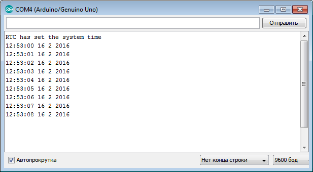
Serial
// sync won't delete else Serial.println ("RTC has set the system time"); // set manually on 02/16/2016 12:53 TimeElements te; te.Second = 0; // seconds te.Minute = 53; // minutes te.Hour = 12; // hours te.Day = 16; // day te.Month = 2; // month te.Year = 2016 - 1970; // the year in the library is counted from 1970 time_t timeVal = makeTime (te); RTC .set (timeVal); setTime (timeVal); ) void loop() (digitalClockDisplay (); // time output delay (1000);) void digitalClockDisplay () ( Serial
Serial.print (""); Serial.print (day ()); Serial.print (""); Serial.print (month ()); Serial.print (""); Serial.print (year ()); Serial
// display time after ":"
Serial.print (":"); if (digits< 10)
Serial.print ("0"); Serial.print (digits); )
... Installation from"Port Monitor"
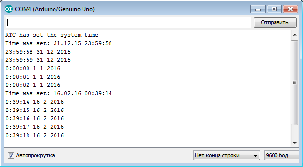
More accurate time setting option. The time is set through the "port monitor" during the controller operation.
We open the monitor, enter the data in the required format, look at the reference clock, catch the moment and silk “send”.
Sample program code
// format for indicating the current time "DD.MM.YY hh: mm: ss"
// where DD - day, MM - month, YY - year, hh - hours, mm - minutes, ss - seconds
// YY - from 00 to 99 for 2000-2099#include #include bool isTimeSet = false; // flag indicating whether the date has already been set void setup
() {
Serial.begin (9600); while (! Serial
) ; // For Leonardo board only setSyncProvider (RTC .get); // get time from RTC if (timeStatus ()! = timeSet) Serial.println ("Unable to sync with the RTC"); // sync won't delete else Serial.println ("RTC has set the system time"); ) void loop() (if ( Serial.available ()) ( // received a command with time setTimeFromFormatString ( Serial.readStringUntil ("\ n")); isTimeSet = true; // date was set) if (isTimeSet) // if a date was given(digitalClockDisplay (); // time output) delay (1000); ) void digitalClockDisplay () ( Serial.print (hour ()); printDigits (minute ()); printDigits (second ()); Serial.print (""); Serial.print (day ()); Serial.print (""); Serial.print (month ()); Serial.print (""); Serial.print (year ()); Serial.println (); ) void printDigits (int digits) ( // display time after ":"
Serial.print (":"); if (digits< 10)
Serial.print ("0"); Serial.print (digits); ) void setTimeFromFormatString (String time) ( //DD.MM.YY hh: mm: ss int day = time.substring (0, 2) .toInt (); int month = time.substring (3, 5) .toInt (); int year = time.substring (6, 8) .toInt (); int hours = time.substring (9, 11) .toInt (); int minutes = time.substring (12, 14) .toInt (); int seconds = time.substring (15, 17) .toInt (); TimeElements te; te.Second = seconds; te.Minute = minutes; te.Hour = hours; te.Day = day; te.Month = month; te.Year = year + 30; // the year in the library is counted from 1970. We want from 2000 time_t timeVal = makeTime (te); RTC .set (timeVal); setTime (timeVal); )
 Buy in Russia
/ * Next, we transfer the address packet (device address). The contents of the package are loaded into the TWDR register * /
TWDR = 0xd0; / * 0b1101000 + 0 - address + write bit * /
/ * Reset the flag for transferring information * /
TWCR = (1<
/ * Waiting for the flag to be set * /
while (! (TWCR & (1<
/ * pass the register to which we will refer * /
TWDR = reg;
TWCR = (1<
while (! (TWCR & (1<
/ * Pass information to be written to the register byte * /
TWDR = time;
TWCR = (1<
while (! (TWCR & (1<
/ * form the STOP state * /
TWCR = (1<
}
In this function, we transferred three bytes, the device address, the register address and a byte of information to write to this register and formed the STOP state.
The last read function remains. Below is the reading format.
This function transfers the device address byte + write bit, the register address byte for setting the pointer to it, the POVSTAR condition is fulfilled, the device address byte + read bit is transferred, the register whose address we transferred earlier is transferred.
If we refer to the clock in the read format, then when the clock is accessed again, the pointer is shifted one byte down, including 56 bytes of RAM, from 00H to 3FH. Upon reaching the last address, the pointer jumps to address 00.
/ * Function for reading data from DS1307 * /
uint8_t read_DS1307 (uint8_t reg)/ * Pass the register address * /
{
uint8_t time;
/ * form the START state * /
TWCR = (1<
while (! (TWCR & (1<
TWDR = 0xd0; / * Pass address + write bit * /
TWCR = (1<
while (! (TWCR & (1<
TWDR = reg; / * Register address * /
TWCR = (1<
while (! (TWCR & (1<
/ * form the POSTAR state * /
TWCR = (1<
while (! (TWCR & (1<
TWDR = 0xd1; / * Pass address + read bit * /
TWCR = (1<
while (! (TWCR & (1<
/ * read data * /
TWCR = (1<
while (! (TWCR & (1<
/ * form the STOP state * /
TWCR = (1<
return time;
}
So above we have written three functions that we need to work with the clock. Using these functions, we will launch the program in Proteus. Let's display, for example, the date.
#include
#include
uint8_t time;
void init_DS1307 (void);
uint8_t read_DS1307 (uint8_t reg);
void write_DS1307 (uint8_t reg, uint8_t time);
int main (void)
{
DDRC = 0x00; / * Set port as input * /
PORTC = 0xFF; / * Pull up resistance * /
init_DS1307;
while (1)
{
_delay_ms (50);
read_DS1307 (0 × 04); / * Read date register * /
}
}
Below is the result of executing the program reading the date.
In the debugger window I2C
you can see that first the address of the register is sent to the RTC (green circle), in this case 04, which is responsible for the date of the month, and then the clock sends the answer 21 (red circle).
When we start the clock in the hardware, we will need to enter the present time. Below is an example of a program for changing the minutes.
while (1)
{
_delay_ms (500);
read_DS1307 (0x01); / * Read the minute * /
_delay_ms (500);
write_DS1307 (0x01,15); / * Write down the required minute * /
_delay_ms (500);
read_DS1307 (0x01); / * Read the minute * /
}
The figure shows that first there is a call to register 01, minute 23 is read. Next, we use the write function, and enter the value 15. At the next read function, we have the value 15 on the clock display.
Well, the last example of the program is the output of the values of all registers.
while (1)
{
delay_ms (500);
read_DS1307 (0x00);
_delay_ms (500);
read_DS1307 (0x01);
_delay_ms (500);
read_DS1307 (0 × 02);
_delay_ms (500);
read_DS1307 (0 × 03);
_delay_ms (500);
read_DS1307 (0 × 04);
_delay_ms (500);
read_DS1307 (0 × 05);
_delay_ms (500);
read_DS1307 (0x06);
_delay_ms (500);
}
The figure below shows that the data of 7 registers was displayed.
The source with the project is attached:
(Downloaded: 341 people)
That's all. Let's connect the clock in hardware, display the time on the indicator and get acquainted with the binary-decimal format for working with the clock. Goodbye to everyone.
DS1307 Real Time Clock Module
Tiny RTC I2C module 24C32 memory DS1307 clock
A small module that performs the functions of a real time clock. It is based on the DS1307ZN + microcircuit. Continuous timing is due to autonomous power supply from the battery installed in the module. The module also contains 32 Kbyte EEPROM memory, which retains information when all types of power are turned off. Memory and clock are linked by a common I2C interface bus. I2C bus signals are output to the module contacts. When an external power supply is connected, the battery is recharged through a primitive recharging circuit. There is space on the board for mounting a DS18B20 digital temperature sensor. It is not included in the package.
The use of this device occurs when measuring time intervals of more than a week with devices based on a microcontroller. It is unjustified and often impossible to use the MK's own resources for this purpose. It is expensive to provide uninterrupted power supply for a long time; it is impossible to install a battery to power the MK because of the significant current consumption. This is where the DS1307 real-time clock module comes to the rescue.
Also, the DS1307 real-time clock module, thanks to its own memory, allows you to record data from events that occur several times a day, for example, temperature measurements. The event log is then read from the module memory. These capabilities allow the module to be used as part of an autonomous automatic weather station or for climate research in hard-to-reach places: caves, rock tops. It becomes possible to register tenso parameters of architectural structures, for example, bridge supports and others. When equipping the device with radio communication, it is enough to install it in the surveyed area.
Specifications
Supply voltage 5 V
Dimensions 27 x 28 x 8.4mm
Electrical diagram
The device communicates with the device electronics using SCL and SDA signals. IC2 is a real time clock. Capacitors C1 and C2 reduce noise on the VCC power line. Resistors R2 and R3 ensure the SCL and SDA signals are at the correct level. IC2's pin 7 outputs a 1 Hz square wave signal SQ. It is used to test the functionality of MS IC2. Components R4, R5, R6, VD1 provide recharging of the BAT1 battery. For data storage, the DS1307 real-time clock module contains IC1, a non-volatile memory. US1 - temperature sensor. Signals of the module and power lines are routed to connectors JP1 and P1.
Data bus
I2C is a standard serial interface with two signal lines SCL, SDA and a common wire. The interface lines form a bus. Several microcircuits can be connected to the I2C interface lines, not only the microcircuits of the module. To identify the microcircuit on the bus, namely, writing data to the required MS and determining from which MS the data is coming. Each microcircuit has a unique address for the laid bus. DS1307 has Address 0x68. It is recorded at the factory. The memory chip has an address of 0x50. The Arduino software includes a software library that provides I2C support.
Real time clock microcircuit
DS1307 has low power consumption, communicates with other devices via I2C interface, and contains 56 bytes of memory. Contains a clock and a calendar until 2100. The real-time clock microcircuit provides other devices with information about the present moment: seconds, minutes, hours, day of the week, date. The number of days in each month is counted automatically. There is a compensation function for leap years. There is a flag to define whether the clock is running in 24-hour mode or 12-hour mode. To operate in 12-hour mode, the microcircuit has a bit from which data is read for transmission about a period of time: before or after lunch.
Long-term memory chip
Illustration of the DS1307 real-time clock module from the battery side with the U1 temperature sensor installed.
Battery
The holder on the back of the board holds a CR2032 lithium disk battery. It is available from many manufacturers, such as one manufactured by GP, which provides 3.6 V and 210 mAh discharge current. The battery is recharged when the power is turned on; this is the mode of operation of a lithium battery that we encounter on the motherboard of a computer.
Recharging the battery
Software
For the module to work as part of the Arduino, an outdated library from the Adafruit website called RTCLib is quite suitable. The sketch is called DS1307.pde. There is an updated version. Download the archive, unpack it, rename and copy the library to your Arduino library directory.
Connecting to Arduino Mega
To do this, use sketches.
SetRTC sets the time in hours according to the time shown in the sketch.
GetRTC displays the time.
Both sketches require the Wire library and define an I2C address. To set the clock address on the I2C bus, use this I2C scanner.
Arduino Mega connection.
Connect SCL and SDA to the corresponding pins 21 and 20 on the Arduino Mega 2560. Connect the power.
Arduino Uno connection
Set time in SetRTC sketch and upload to Arduino. Then press the reset button to set the clock. Now download the GetRTC sketch. Open the serial monitor and watch. There is a special time library. It has many different functions that can be useful depending on the situation. To set the time using the library you need to download. When using a sketch, you can synchronize the real-time clock with the clock of your personal computer.
Vbat- battery input for any standard 3 Volt lithium cell or other power source. For normal operation, the battery voltage must be maintained between 2.5 and 3.5 V. The level at which access to the real time clock and user RAM is denied is internally set to 1.25 x Vbat. A lithium battery with a capacity of 35 mAh or more is sufficient to power the DS1307 for more than 10 years without power.
SCL(Serial Clock Input) - SCL is used to synchronize data transmission over the serial interface.
SDA(Serial Data I / O) - SDA - data I / O for 2-wire serial interface. This is an open drain output that requires an external pull-up resistor.
SQW / OUT(Square Wave / Output Driver) - When the SQWE bit is set to 1, the SQW / OUT outputs a square wave of one of four frequencies: 1 Hz, 4 kHz, 8 kHz, 32 kHz. The SQW / OUT pin is open drain and requires an external pull-up resistor.
X1, X2- pins for connecting a standard crystal of quartz 32.768 kHz. The internal circuit of the generator is designed to operate with a crystal having a nominal capacitance (CL) of 12.5 pF.
GND- Land.
VCC- power supply 5 volts.
DS1307 works as a slave on the serial bus. To access it, you need to set the state START and transmit the device identification code followed by the register address. Subsequent registers can be accessed sequentially until the state is set. STOP... When VCC falls below 1.25 x Vbat, the device stops communicating and resets the address counter. During this time, it will not respond to input signals to prevent the recording of erroneous information. When VCC drops below Vbat, the device switches to low power storage mode. When powered on, the unit switches power from battery to VCC when the supply voltage exceeds Vbat + 0.2V, and reacts to input signals when VCC will become more than 1.25 x Vbat. When the power is within normal limits, the device is fully accessible and data can be written and read. When a 3V battery is connected to the device and VCC is lower than 1.25 x Vbat, reading and writing is prohibited. However, the countdown works. When VCC drops below Vbat, the RAM and timing power supply switches to an external 3 V battery.
Time and date information is obtained by reading the corresponding registers. The clock registers are shown in the table below. Time and calendar are set or initialized by writing bytes to the appropriate registers. The contents of the time and calendar registers are stored in BCD (BCD) format, therefore, before displaying information on the LCD display or seven-segment indicator, it is necessary to convert the binary-decimal code to a binary or ANSII code.
Bit 7 of register 0 is the Clock Halt bit. When this bit is set to 1, the generator is stopped. When reset to zero, the generator is running and the clock is counting the time.
DS1307 can operate in 12-hour or 24-hour mode. Bit 6 of the clock register specifies one of these modes. When it is 1, the 12 hour mode is set. In 12 o'clock mode, bit 5 high indicates afternoon time. In 24-hour mode, bit 5 is the second bit of 10 hours (20-23 hours).
The DS1307 control register is designed to control the operation of the output SQW / OUT... Bit OUT- output control. This bit controls the output level on the pin. SQW / OUT when the generation of the meander is disabled. If SQWE = 0, the logic level on the pin SQW / OUT equals 1 if OUT= 1, and 0 - if OUT = 0. SQWE- Resolution of the meander. When this bit is set to 1, square wave generation is enabled. The square wave frequency depends on the values of the RS0 and RS1 bits. These bits control the frequency of the square wave when it is enabled. The table below shows the frequencies that can be specified by the RS bits.
DS1307 supports bi-directional 2-wire bus and communication protocol. The device that sends data to the bus is called a transmitter, and the device that receives the data is called a receiver. The device that controls the transmission is called the master. Devices controlled by the master are slaves. The bus must be controlled by a master that generates sequential clocks (SCL), controls access to the bus, and generates START and STOP states. DS1307 acts as a slave on a 2-wire bus.
To work with DS1307, it is necessary to organize the read function from the microcircuit and the write function.
1. DS1307 recording mode... Serial data and clocks are received via SDA and SCL. After the transmission of each byte, a confirmation bit is transmitted. ASK... States START and STOP are recognized as the beginning and end of the serial transmission. Address recognition is performed in hardware after receiving the slave address and direction bit. The address byte contains the 7-bit DS1307 address, equal to 1101000, followed by the direction bit (R / W), which when written is 0. After receiving and decrypting the address byte, the DS1307 issues an acknowledgment ASK on the SDA line. After the DS1307 confirms the slave address and write bit, the master transmits the DS1307 register address. This will set the register pointer in DS1307. The master will then start transmitting data bytes to the DS1307, which will acknowledge each byte received. At the end of the recording, the presenter will form a state STOP.
2. Reading mode from DS1307... The first byte is received and processed as in slave receiver mode. However, in this mode, the direction bit will indicate that the transmission direction has been reversed. Serial data is sent over SDA from the DS1307, while serial clocks are sent over SCL from the DS1307. States START and STOP are recognized as the beginning and end of the serial transmission. Address byte - the first byte received after the master has generated a state START... The address byte contains the 7-bit DS1307 address, equal to 1101000, followed by the direction bit (R / W), which when read is 1. After receiving and decrypting the address byte, the DS1307 issues an acknowledgment ASK on the SDA line. The DS1307 then starts transmitting data starting at the register address pointed to by the register pointer. If the register pointer is not written before initiating the read mode, then the first address that is read is the last address remaining in the register pointer. DS1307 should get unacknowledged NOASK to finish reading.
Let's consider the features of working with DS1307 using a simple clock as an example, which will show hours, minutes and seconds. The data will be displayed on a 16x2 LCD display. Two buttons "Hours +" and "Minutes +" will allow you to set the desired time. The Atmega 8 microcontroller is clocked by an internal 1 MHz oscillator, so don't forget to change the fuses. Below is a connection diagram.
The control program includes a set of functions for working with the TWI bus, DS1307 clock, LCD display.
I2CInit - bus initialization;
I2CStart - transmission of the START condition;
I2CStop - transmission of the STOP condition;
I2CWriteByte - data writing;
I2CReadByte - reading data;
DS1307Read - function for reading data from DS1307;
DS1307Write - Function of writing data to DS1307;
lcd_com - sending a command to the LCD;
lcd_data - data transfer to LCD;
lcd_string - function for displaying a string in the LCD;
lcd_num_to_str - function for outputting a character of int type;
lcd_init - LCD initialization.
Below is the program code:
#include #include // Function initialization of the TWI bus void I2CInit (void) (// setting the TWI module TWBR = 2; TWSR = (1<< TWPS1)|(1 << TWPS0); // Предделитель на 64
TWCR |= (1 << TWEN); // Включение модуля TWI
}
void I2CStart(void)
{
// Передача условия СТАРТ
TWCR = (1 << TWINT)|(1 << TWEN)|(1 << TWSTA);
// Ожидание установки флага TWINT
while(!(TWCR & (1 << TWINT)));
}
void I2CStop(void)
{
TWCR = (1 << TWINT)|(1 << TWEN)|(1 << TWSTO); // Передача условия СТОП
while(TWCR & (1 << TWSTO)); // Ожидание завершения передачи условия СТОП
}
// Функция записи данных по шине
uint8_t I2CWriteByte(uint8_t data)
{
TWDR = data; // Загрузка данных в TWDR
TWCR = (1 << TWEN)|(1 << TWINT); // Сброс флага TWINT для начала передачи данных
while(!(TWCR & (1 << TWINT))); // Ожидание завершения передачи
// Проверка статуса
if((TWSR & 0xF8) == 0x18 || (TWSR & 0xF8) == 0x28 || (TWSR & 0xF8) == 0x40)
{
// Если адрес DS1307, биты R/W и данные переданы
// и получено подтверждение
return 1;
}
else
return 0; // ОШИБКА
}
// Функция чтения данных по шине
uint8_t I2CReadByte(uint8_t *data,uint8_t ack)
{
if(ack) // Устанавливаем подтверждение
{
// Возвращаем подтверждение после приема
TWCR |= (1 << TWEA);
}
else
{
// Возвращаем неподтверждение после приема
// Ведомое устройство не получает больше данных
// обычно используется для распознования последнего байта
TWCR &= ~(1 << TWEA);
}
// Разрешение приема данных после сброса TWINT
TWCR |= (1 << TWINT);
while(!(TWCR & (1 << TWINT))); // Ожидание установки флага TWINT
// Проверка статуса
if((TWSR & 0xF8) == 0x58 || (TWSR & 0xF8) == 0x50)
{
// Прием данных и возвращение подтверждения
// или
// Прием данных и возвращение неподтверждения
*data = TWDR; // Читаем данные
return 1;
}
else
return 0; // Ошибка
}
// Функция чтения данных из DS1307
uint8_t DS1307Read(uint8_t address,uint8_t *data)
{
uint8_t res; // Результат
I2CStart(); // СТАРТ
res = I2CWriteByte(0b11010000); // адрес DS1307 + бит W
if(!res) return 0; // ОШИБКА
// Передача адреса необходимого регистра
res = I2CWriteByte(address);
if(!res) return 0; // ОШИБКА
I2CStart(); // Повторный СТАРТ
res = I2CWriteByte(0b11010001); // адрес DS1307 + бит R
if(!res) return 0; // ОШИБКА
// Чтение данных с неподтверждением
res = I2CReadByte(data,0);
if(!res) return 0; // ОШИБКА
I2CStop(); // СТОП
return 1;
}
// Функция записи данных в DS1307
uint8_t DS1307Write(uint8_t address,uint8_t data)
{
uint8_t res; // Результат
I2CStart(); // СТАРТ
res = I2CWriteByte(0b11010000); // адрес DS1307 + бит W
if(!res) return 0; // ОШИБКА
// Передача адреса необходимого регистра
res = I2CWriteByte(address);
if(!res) return 0; // ОШИБКА
res = I2CWriteByte(data); // Запись данных
if(!res) return 0; // ОШИБКА
I2CStop(); // СТОП
return 1;
}
// Функции работы с LCD
#define RS PD0
#define EN PD2
// Функция передачи команды
void lcd_com(unsigned char p)
{
PORTD &= ~(1 << RS); // RS = 0 (запись команд)
PORTD |= (1 << EN); // EN = 1 (начало записи команды в LCD)
PORTD &= 0x0F; PORTD |= (p & 0xF0); // старший нибл
_delay_us(100);
PORTD &= ~(1 << EN); // EN = 0 (конец записи команды в LCD)
_delay_us(100);
PORTD |= (1 << EN); // EN = 1 (начало записи команды в LCD)
PORTD &= 0x0F; PORTD |= (p << 4); // младший нибл
_delay_us(100);
PORTD &= ~(1 << EN); // EN = 0 (конец записи команды в LCD)
_delay_us(100);
}
// Функция передачи данных
void lcd_data(unsigned char p)
{
PORTD |= (1 << RS)|(1 << EN); // RS = 1 (запись данных), EN - 1 (начало записи команды в LCD)
PORTD &= 0x0F; PORTD |= (p & 0xF0); // старший нибл
_delay_us(100);
PORTD &= ~(1 << EN); // EN = 0 (конец записи команды в LCD)
_delay_us(100);
PORTD |= (1 << EN); // EN = 1 (начало записи команды в LCD)
PORTD &= 0x0F; PORTD |= (p << 4); // младший нибл
_delay_us(100);
PORTD &= ~(1 << EN); // EN = 0 (конец записи команды в LCD)
_delay_us(100);
}
// Функция вывода строки на LCD
void lcd_string(unsigned char command, char *string)
{
lcd_com(0x0C);
lcd_com(command);
while(*string != "\0")
{ lcd_data(*string);
string++;
}
}
// Функция вывода переменной
void lcd_num_to_str(unsigned int value, unsigned char nDigit)
{
switch(nDigit)
{
case 4: lcd_data((value/1000)+"0");
case 3: lcd_data(((value/100)%10)+"0");
case 2: lcd_data(((value/10)%10)+"0");
case 1: lcd_data((value%10)+"0");
}
}
// Функция инициализации LCD
void lcd_init(void)
{
PORTD = 0x00;
DDRD = 0xFF;
_delay_ms(50); // Ожидание готовности ЖК-модуля
// Конфигурирование четырехразрядного режима
PORTD |= (1 << PD5);
PORTD &= ~(1 << PD4);
// Активизация четырехразрядного режима
PORTD |= (1 << EN);
PORTD &= ~(1 << EN);
_delay_ms(5);
lcd_com(0x28); // шина 4 бит, LCD - 2 строки
lcd_com(0x08); // полное выключение дисплея
lcd_com(0x01); // очистка дисплея
_delay_us(100);
lcd_com(0x06); // сдвиг курсора вправо
lcd_com(0x0C); // включение дисплея, курсор не видим
}
int main(void)
{
_delay_ms(100);
DDRC = 0x00;
PORTC = 0xFF;
lcd_init(); // Инициализация LCD
I2CInit(); // Инициализация шины I2C
// Запускаем ход часов
uint8_t temp;
DS1307Read(0x00,&temp);
temp &= ~(1 << 7); // обнуляем 7 бит
DS1307Write(0x00,temp);
while(1)
{
unsigned char hour, minute, second, temp;
// Читаем данные и преобразуем из BCD в двоичную систему
DS1307Read(0x00,&temp); // Чтение регистра секунд
second = (((temp & 0xF0) >> 4) * 10) + (temp & 0x0F); DS1307Read (0x01, & temp); // Read the minute register minute = (((temp & 0xF0) >> 4) * 10) + (temp & 0x0F); DS1307Read (0x02, & temp); // Read the clock register hour = (((temp & 0xF0) >> 4) * 10) + (temp & 0x0F); lcd_string (0x81, "" acГ Ѕa DS1307 "); lcd_string (0xC4, "::"); lcd_com (0xC4); lcd_num_to_str (hour, 2); // Display the clock lcd_com (0xC7); lcd_num_to_str (minute, 2); // Display minutes lcd_com (0xCA); lcd_num_to_str (second, 2); // Display seconds if ((PINC & (1<< PC0))==0) // Если нажата кнопка
{
while((PINC & (1 << PC0))==0){} // Ждем отпускания кнопки
hour++; // Увеличиваем часы на 1
if(hour >23) hour = 0; // Convert from binary to BCD and write to DS1307 uint8_t temp; temp = ((hour / 10)<< 4)|(hour%10);
DS1307Write(0x02, temp);
_delay_ms(100);
}
if((PINC & (1 << PC1))==0) // Если нажата кнопка
{
while((PINC & (1 << PC1))==0){} // Ждем отпускания кнопки
minute++; // Увеличиваем минуты на 1
if(minute >59) minute = 0; // Convert from binary to BCD and write to DS1307 uint8_t temp; temp = ((minute / 10)<< 4)|(minute%10);
DS1307Write(0x01, temp);
_delay_ms(100);
}
}
}
The module considered in the article contains two microcircuits at once: DS1307 (real time clock with I2C interface) and AT24C32 (32K bit EEPROM memory microcircuit).
In this article, we will consider the operation of only the DS1307 real-time clock microcircuit.
Main technical characteristics:
Counting real time in seconds, minutes, hours, dates of the month, months, days of the week and years, taking into account the highness of the current year up to 2100.
56 bytes of non-volatile RAM for data storage
2-wire serial interface
Programmable square-wave generator. Can output 1HZ, 4.096KHZ, 8.192KHZ and 32.768KHZ.
Automatic detection of disconnection of the main power supply and connection of the backup
24 hour and 12 hour mode
Consumption no more than 500 nA when powered by a backup battery at a temperature of 25C °
The microcircuit is available in eight-pin DIP and SOIC packages. The pinout is the same for everyone. Below are the lines from the datasheet for completeness.
Chip documentation (datasheet)
Pin assignment:
. X1, X2- Serves to connect a 32.768 kHz crystal resonator
. Vbat- Input for any standard 3V lithium battery or other power source. For normal operation of DS1307, the battery voltage must be in the range of 2.0 ... 3.5 V.
for more than 10 years at a temperature of 25 ° C.
. GND- general minus
. Vcc- This is a +5 V input. When the supply voltage is higher than 1.25 * VBAT, the device is fully accessible and data can be read and written. When a 3V battery is connected to the device and the Vcc is lower than 1.25 * VBAT, reading and writing is prohibited, but the timing function continues to work. As soon as Vcc drops below VBAT, RAM and RTC switch to battery powered VBAT.
. SQW / OUT- Output signal with rectangular pulses.
. SCL- (Serial Clock Input) - used to synchronize data over the serial interface.
. SDA- (Serial Data Input / Output) - Input / output pin for two-wire serial interface.
Working with the SQW / OUT pin.
First, let's look at the structure of DS1307 registers.
The structure of registers of the DS1307 microcircuit
We are interested in the "Control register" located at 0x7, since it determines the behavior of the SQW / OUT pin.
If the SQWE bit = 1. then the formation of rectangular pulses begins, if SQWE = 0, then the value of the OUT bit will be at the output of the output.
Bits RS0 and RS1 are responsible for the pulse frequency, namely:
RS0
RS1
Frequency
0
0
1 Hz
0
1
4.096 kHz
1
0
8.192 kHz
1
1
32.768 kHz
Let's give an example:
If we need to start forming rectangular pulses with a frequency of 1 Hz, then we need to send a byte 00010000 or 0x10 in hexadecimal notation to the 0x7 register of the microcircuit, which has the address 0x68.
Using the library Wire.h, it can be done like this:
Wire .beginTransmission (0x68); Wire .write (0x7); Wire .write (0x10); Wire .endTransmission ();
Connecting to Arduino:
The pins responsible for the I2C interface on Arduino boards based on different controllers are different.
Required libraries:
to work with DS1307: http://www.pjrc.com/teensy/td_libs_DS1307RTC.html
for working with time: http://www.pjrc.com/teensy/td_libs_Time.html
Time setting
... Manually in code
The time is set manually in the program code and poured into the Arduino board. This method is not the most accurate. compilation and loading times can take different periods of time.
Sample program code
#include #include void setup
() {
Serial.begin (9600); while (! Serial
) ; // For Leonardo board only
// get time from RTC
Serial
// sync won't delete else Serial.println ("RTC has set the system time"); // set manually on 02/16/2016 12:53 TimeElements te; te.Second = 0; // seconds te.Minute = 53; // minutes te.Hour = 12; // hours te.Day = 16; // day te.Month = 2; // month te.Year = 2016 - 1970; // the year in the library is counted from 1970 time_t timeVal = makeTime (te); RTC .set (timeVal); setTime (timeVal); ) void loop() (digitalClockDisplay (); // time output delay (1000);) void digitalClockDisplay () ( Serial
Serial.print (""); Serial.print (day ()); Serial.print (""); Serial.print (month ()); Serial.print (""); Serial.print (year ()); Serial
// display time after ":"
Serial.print (":"); if (digits< 10)
Serial.print ("0"); Serial.print (digits); )
... Installation from"Port Monitor"
More accurate time setting option. The time is set through the "port monitor" during the controller operation.
We open the monitor, enter the data in the required format, look at the reference clock, catch the moment and silk “send”.
Sample program code
// format for indicating the current time "DD.MM.YY hh: mm: ss"
// where DD - day, MM - month, YY - year, hh - hours, mm - minutes, ss - seconds
// YY - from 00 to 99 for 2000-2099#include #include bool isTimeSet = false; // flag indicating whether the date has already been set void setup
() {
Serial.begin (9600); while (! Serial
) ; // For Leonardo board only setSyncProvider (RTC .get); // get time from RTC if (timeStatus ()! = timeSet) Serial.println ("Unable to sync with the RTC"); // sync won't delete else Serial.println ("RTC has set the system time"); ) void loop() (if ( Serial.available ()) ( // received a command with time setTimeFromFormatString ( Serial.readStringUntil ("\ n")); isTimeSet = true; // date was set) if (isTimeSet) // if a date was given(digitalClockDisplay (); // time output) delay (1000); ) void digitalClockDisplay () ( Serial.print (hour ()); printDigits (minute ()); printDigits (second ()); Serial.print (""); Serial.print (day ()); Serial.print (""); Serial.print (month ()); Serial.print (""); Serial.print (year ()); Serial.println (); ) void printDigits (int digits) ( // display time after ":"
Serial.print (":"); if (digits< 10)
Serial.print ("0"); Serial.print (digits); ) void setTimeFromFormatString (String time) ( //DD.MM.YY hh: mm: ss int day = time.substring (0, 2) .toInt (); int month = time.substring (3, 5) .toInt (); int year = time.substring (6, 8) .toInt (); int hours = time.substring (9, 11) .toInt (); int minutes = time.substring (12, 14) .toInt (); int seconds = time.substring (15, 17) .toInt (); TimeElements te; te.Second = seconds; te.Minute = minutes; te.Hour = hours; te.Day = day; te.Month = month; te.Year = year + 30; // the year in the library is counted from 1970. We want from 2000 time_t timeVal = makeTime (te); RTC .set (timeVal); setTime (timeVal); )
Buy in Russia
while (! (TWCR & (1<
/ * Pass information to be written to the register byte * /
TWDR = time;
TWCR = (1<
while (! (TWCR & (1<
/ * form the STOP state * /
TWCR = (1<
}
In this function, we transferred three bytes, the device address, the register address and a byte of information to write to this register and formed the STOP state.
The last read function remains. Below is the reading format.
This function transfers the device address byte + write bit, the register address byte for setting the pointer to it, the POVSTAR condition is fulfilled, the device address byte + read bit is transferred, the register whose address we transferred earlier is transferred.
If we refer to the clock in the read format, then when the clock is accessed again, the pointer is shifted one byte down, including 56 bytes of RAM, from 00H to 3FH. Upon reaching the last address, the pointer jumps to address 00.
/ * Function for reading data from DS1307 * /
uint8_t read_DS1307 (uint8_t reg)/ * Pass the register address * /
{
uint8_t time;
/ * form the START state * /
TWCR = (1<
while (! (TWCR & (1<
TWDR = 0xd0; / * Pass address + write bit * /
TWCR = (1<
while (! (TWCR & (1<
TWDR = reg; / * Register address * /
TWCR = (1<
while (! (TWCR & (1<
/ * form the POSTAR state * /
TWCR = (1<
while (! (TWCR & (1<
TWDR = 0xd1; / * Pass address + read bit * /
TWCR = (1<
while (! (TWCR & (1<
/ * read data * /
TWCR = (1<
while (! (TWCR & (1<
/ * form the STOP state * /
TWCR = (1<
return time;
}
So above we have written three functions that we need to work with the clock. Using these functions, we will launch the program in Proteus. Let's display, for example, the date.
#include
#include
uint8_t time;
void init_DS1307 (void);
uint8_t read_DS1307 (uint8_t reg);
void write_DS1307 (uint8_t reg, uint8_t time);
int main (void)
{
DDRC = 0x00; / * Set port as input * /
PORTC = 0xFF; / * Pull up resistance * /
init_DS1307;
while (1)
{
_delay_ms (50);
read_DS1307 (0 × 04); / * Read date register * /
}
}
Below is the result of executing the program reading the date.
In the debugger window I2C
you can see that first the address of the register is sent to the RTC (green circle), in this case 04, which is responsible for the date of the month, and then the clock sends the answer 21 (red circle).
When we start the clock in the hardware, we will need to enter the present time. Below is an example of a program for changing the minutes.
while (1)
{
_delay_ms (500);
read_DS1307 (0x01); / * Read the minute * /
_delay_ms (500);
write_DS1307 (0x01,15); / * Write down the required minute * /
_delay_ms (500);
read_DS1307 (0x01); / * Read the minute * /
}
The figure shows that first there is a call to register 01, minute 23 is read. Next, we use the write function, and enter the value 15. At the next read function, we have the value 15 on the clock display.
Well, the last example of the program is the output of the values of all registers.
while (1)
{
delay_ms (500);
read_DS1307 (0x00);
_delay_ms (500);
read_DS1307 (0x01);
_delay_ms (500);
read_DS1307 (0 × 02);
_delay_ms (500);
read_DS1307 (0 × 03);
_delay_ms (500);
read_DS1307 (0 × 04);
_delay_ms (500);
read_DS1307 (0 × 05);
_delay_ms (500);
read_DS1307 (0x06);
_delay_ms (500);
}
The figure below shows that the data of 7 registers was displayed.
The source with the project is attached:
(Downloaded: 341 people)
That's all. Let's connect the clock in hardware, display the time on the indicator and get acquainted with the binary-decimal format for working with the clock. Goodbye to everyone.
DS1307 Real Time Clock Module
Tiny RTC I2C module 24C32 memory DS1307 clock
A small module that performs the functions of a real time clock. It is based on the DS1307ZN + microcircuit. Continuous timing is due to autonomous power supply from the battery installed in the module. The module also contains 32 Kbyte EEPROM memory, which retains information when all types of power are turned off. Memory and clock are linked by a common I2C interface bus. I2C bus signals are output to the module contacts. When an external power supply is connected, the battery is recharged through a primitive recharging circuit. There is space on the board for mounting a DS18B20 digital temperature sensor. It is not included in the package.
The use of this device occurs when measuring time intervals of more than a week with devices based on a microcontroller. It is unjustified and often impossible to use the MK's own resources for this purpose. It is expensive to provide uninterrupted power supply for a long time; it is impossible to install a battery to power the MK because of the significant current consumption. This is where the DS1307 real-time clock module comes to the rescue.
Also, the DS1307 real-time clock module, thanks to its own memory, allows you to record data from events that occur several times a day, for example, temperature measurements. The event log is then read from the module memory. These capabilities allow the module to be used as part of an autonomous automatic weather station or for climate research in hard-to-reach places: caves, rock tops. It becomes possible to register tenso parameters of architectural structures, for example, bridge supports and others. When equipping the device with radio communication, it is enough to install it in the surveyed area.
Specifications
Supply voltage 5 V
Dimensions 27 x 28 x 8.4mm
Electrical diagram
The device communicates with the device electronics using SCL and SDA signals. IC2 is a real time clock. Capacitors C1 and C2 reduce noise on the VCC power line. Resistors R2 and R3 ensure the SCL and SDA signals are at the correct level. IC2's pin 7 outputs a 1 Hz square wave signal SQ. It is used to test the functionality of MS IC2. Components R4, R5, R6, VD1 provide recharging of the BAT1 battery. For data storage, the DS1307 real-time clock module contains IC1, a non-volatile memory. US1 - temperature sensor. Signals of the module and power lines are routed to connectors JP1 and P1.
Data bus
I2C is a standard serial interface with two signal lines SCL, SDA and a common wire. The interface lines form a bus. Several microcircuits can be connected to the I2C interface lines, not only the microcircuits of the module. To identify the microcircuit on the bus, namely, writing data to the required MS and determining from which MS the data is coming. Each microcircuit has a unique address for the laid bus. DS1307 has Address 0x68. It is recorded at the factory. The memory chip has an address of 0x50. The Arduino software includes a software library that provides I2C support.
Real time clock microcircuit
DS1307 has low power consumption, communicates with other devices via I2C interface, and contains 56 bytes of memory. Contains a clock and a calendar until 2100. The real-time clock microcircuit provides other devices with information about the present moment: seconds, minutes, hours, day of the week, date. The number of days in each month is counted automatically. There is a compensation function for leap years. There is a flag to define whether the clock is running in 24-hour mode or 12-hour mode. To operate in 12-hour mode, the microcircuit has a bit from which data is read for transmission about a period of time: before or after lunch.
Long-term memory chip
Illustration of the DS1307 real-time clock module from the battery side with the U1 temperature sensor installed.
Battery
The holder on the back of the board holds a CR2032 lithium disk battery. It is available from many manufacturers, such as one manufactured by GP, which provides 3.6 V and 210 mAh discharge current. The battery is recharged when the power is turned on; this is the mode of operation of a lithium battery that we encounter on the motherboard of a computer.
Recharging the battery
Software
For the module to work as part of the Arduino, an outdated library from the Adafruit website called RTCLib is quite suitable. The sketch is called DS1307.pde. There is an updated version. Download the archive, unpack it, rename and copy the library to your Arduino library directory.
Connecting to Arduino Mega
To do this, use sketches.
SetRTC sets the time in hours according to the time shown in the sketch.
GetRTC displays the time.
Both sketches require the Wire library and define an I2C address. To set the clock address on the I2C bus, use this I2C scanner.
Arduino Mega connection.
Connect SCL and SDA to the corresponding pins 21 and 20 on the Arduino Mega 2560. Connect the power.
Arduino Uno connection
Set time in SetRTC sketch and upload to Arduino. Then press the reset button to set the clock. Now download the GetRTC sketch. Open the serial monitor and watch. There is a special time library. It has many different functions that can be useful depending on the situation. To set the time using the library you need to download. When using a sketch, you can synchronize the real-time clock with the clock of your personal computer.
Vbat- battery input for any standard 3 Volt lithium cell or other power source. For normal operation, the battery voltage must be maintained between 2.5 and 3.5 V. The level at which access to the real time clock and user RAM is denied is internally set to 1.25 x Vbat. A lithium battery with a capacity of 35 mAh or more is sufficient to power the DS1307 for more than 10 years without power.
SCL(Serial Clock Input) - SCL is used to synchronize data transmission over the serial interface.
SDA(Serial Data I / O) - SDA - data I / O for 2-wire serial interface. This is an open drain output that requires an external pull-up resistor.
SQW / OUT(Square Wave / Output Driver) - When the SQWE bit is set to 1, the SQW / OUT outputs a square wave of one of four frequencies: 1 Hz, 4 kHz, 8 kHz, 32 kHz. The SQW / OUT pin is open drain and requires an external pull-up resistor.
X1, X2- pins for connecting a standard crystal of quartz 32.768 kHz. The internal circuit of the generator is designed to operate with a crystal having a nominal capacitance (CL) of 12.5 pF.
GND- Land.
VCC- power supply 5 volts.
DS1307 works as a slave on the serial bus. To access it, you need to set the state START and transmit the device identification code followed by the register address. Subsequent registers can be accessed sequentially until the state is set. STOP... When VCC falls below 1.25 x Vbat, the device stops communicating and resets the address counter. During this time, it will not respond to input signals to prevent the recording of erroneous information. When VCC drops below Vbat, the device switches to low power storage mode. When powered on, the unit switches power from battery to VCC when the supply voltage exceeds Vbat + 0.2V, and reacts to input signals when VCC will become more than 1.25 x Vbat. When the power is within normal limits, the device is fully accessible and data can be written and read. When a 3V battery is connected to the device and VCC is lower than 1.25 x Vbat, reading and writing is prohibited. However, the countdown works. When VCC drops below Vbat, the RAM and timing power supply switches to an external 3 V battery.
Time and date information is obtained by reading the corresponding registers. The clock registers are shown in the table below. Time and calendar are set or initialized by writing bytes to the appropriate registers. The contents of the time and calendar registers are stored in BCD (BCD) format, therefore, before displaying information on the LCD display or seven-segment indicator, it is necessary to convert the binary-decimal code to a binary or ANSII code.
Bit 7 of register 0 is the Clock Halt bit. When this bit is set to 1, the generator is stopped. When reset to zero, the generator is running and the clock is counting the time.
DS1307 can operate in 12-hour or 24-hour mode. Bit 6 of the clock register specifies one of these modes. When it is 1, the 12 hour mode is set. In 12 o'clock mode, bit 5 high indicates afternoon time. In 24-hour mode, bit 5 is the second bit of 10 hours (20-23 hours).
The DS1307 control register is designed to control the operation of the output SQW / OUT... Bit OUT- output control. This bit controls the output level on the pin. SQW / OUT when the generation of the meander is disabled. If SQWE = 0, the logic level on the pin SQW / OUT equals 1 if OUT= 1, and 0 - if OUT = 0. SQWE- Resolution of the meander. When this bit is set to 1, square wave generation is enabled. The square wave frequency depends on the values of the RS0 and RS1 bits. These bits control the frequency of the square wave when it is enabled. The table below shows the frequencies that can be specified by the RS bits.
DS1307 supports bi-directional 2-wire bus and communication protocol. The device that sends data to the bus is called a transmitter, and the device that receives the data is called a receiver. The device that controls the transmission is called the master. Devices controlled by the master are slaves. The bus must be controlled by a master that generates sequential clocks (SCL), controls access to the bus, and generates START and STOP states. DS1307 acts as a slave on a 2-wire bus.
To work with DS1307, it is necessary to organize the read function from the microcircuit and the write function.
1. DS1307 recording mode... Serial data and clocks are received via SDA and SCL. After the transmission of each byte, a confirmation bit is transmitted. ASK... States START and STOP are recognized as the beginning and end of the serial transmission. Address recognition is performed in hardware after receiving the slave address and direction bit. The address byte contains the 7-bit DS1307 address, equal to 1101000, followed by the direction bit (R / W), which when written is 0. After receiving and decrypting the address byte, the DS1307 issues an acknowledgment ASK on the SDA line. After the DS1307 confirms the slave address and write bit, the master transmits the DS1307 register address. This will set the register pointer in DS1307. The master will then start transmitting data bytes to the DS1307, which will acknowledge each byte received. At the end of the recording, the presenter will form a state STOP.
2. Reading mode from DS1307... The first byte is received and processed as in slave receiver mode. However, in this mode, the direction bit will indicate that the transmission direction has been reversed. Serial data is sent over SDA from the DS1307, while serial clocks are sent over SCL from the DS1307. States START and STOP are recognized as the beginning and end of the serial transmission. Address byte - the first byte received after the master has generated a state START... The address byte contains the 7-bit DS1307 address, equal to 1101000, followed by the direction bit (R / W), which when read is 1. After receiving and decrypting the address byte, the DS1307 issues an acknowledgment ASK on the SDA line. The DS1307 then starts transmitting data starting at the register address pointed to by the register pointer. If the register pointer is not written before initiating the read mode, then the first address that is read is the last address remaining in the register pointer. DS1307 should get unacknowledged NOASK to finish reading.
Let's consider the features of working with DS1307 using a simple clock as an example, which will show hours, minutes and seconds. The data will be displayed on a 16x2 LCD display. Two buttons "Hours +" and "Minutes +" will allow you to set the desired time. The Atmega 8 microcontroller is clocked by an internal 1 MHz oscillator, so don't forget to change the fuses. Below is a connection diagram.
The control program includes a set of functions for working with the TWI bus, DS1307 clock, LCD display.
I2CInit - bus initialization;
I2CStart - transmission of the START condition;
I2CStop - transmission of the STOP condition;
I2CWriteByte - data writing;
I2CReadByte - reading data;
DS1307Read - function for reading data from DS1307;
DS1307Write - Function of writing data to DS1307;
lcd_com - sending a command to the LCD;
lcd_data - data transfer to LCD;
lcd_string - function for displaying a string in the LCD;
lcd_num_to_str - function for outputting a character of int type;
lcd_init - LCD initialization.
Below is the program code:
#include #include // Function initialization of the TWI bus void I2CInit (void) (// setting the TWI module TWBR = 2; TWSR = (1<< TWPS1)|(1 << TWPS0); // Предделитель на 64
TWCR |= (1 << TWEN); // Включение модуля TWI
}
void I2CStart(void)
{
// Передача условия СТАРТ
TWCR = (1 << TWINT)|(1 << TWEN)|(1 << TWSTA);
// Ожидание установки флага TWINT
while(!(TWCR & (1 << TWINT)));
}
void I2CStop(void)
{
TWCR = (1 << TWINT)|(1 << TWEN)|(1 << TWSTO); // Передача условия СТОП
while(TWCR & (1 << TWSTO)); // Ожидание завершения передачи условия СТОП
}
// Функция записи данных по шине
uint8_t I2CWriteByte(uint8_t data)
{
TWDR = data; // Загрузка данных в TWDR
TWCR = (1 << TWEN)|(1 << TWINT); // Сброс флага TWINT для начала передачи данных
while(!(TWCR & (1 << TWINT))); // Ожидание завершения передачи
// Проверка статуса
if((TWSR & 0xF8) == 0x18 || (TWSR & 0xF8) == 0x28 || (TWSR & 0xF8) == 0x40)
{
// Если адрес DS1307, биты R/W и данные переданы
// и получено подтверждение
return 1;
}
else
return 0; // ОШИБКА
}
// Функция чтения данных по шине
uint8_t I2CReadByte(uint8_t *data,uint8_t ack)
{
if(ack) // Устанавливаем подтверждение
{
// Возвращаем подтверждение после приема
TWCR |= (1 << TWEA);
}
else
{
// Возвращаем неподтверждение после приема
// Ведомое устройство не получает больше данных
// обычно используется для распознования последнего байта
TWCR &= ~(1 << TWEA);
}
// Разрешение приема данных после сброса TWINT
TWCR |= (1 << TWINT);
while(!(TWCR & (1 << TWINT))); // Ожидание установки флага TWINT
// Проверка статуса
if((TWSR & 0xF8) == 0x58 || (TWSR & 0xF8) == 0x50)
{
// Прием данных и возвращение подтверждения
// или
// Прием данных и возвращение неподтверждения
*data = TWDR; // Читаем данные
return 1;
}
else
return 0; // Ошибка
}
// Функция чтения данных из DS1307
uint8_t DS1307Read(uint8_t address,uint8_t *data)
{
uint8_t res; // Результат
I2CStart(); // СТАРТ
res = I2CWriteByte(0b11010000); // адрес DS1307 + бит W
if(!res) return 0; // ОШИБКА
// Передача адреса необходимого регистра
res = I2CWriteByte(address);
if(!res) return 0; // ОШИБКА
I2CStart(); // Повторный СТАРТ
res = I2CWriteByte(0b11010001); // адрес DS1307 + бит R
if(!res) return 0; // ОШИБКА
// Чтение данных с неподтверждением
res = I2CReadByte(data,0);
if(!res) return 0; // ОШИБКА
I2CStop(); // СТОП
return 1;
}
// Функция записи данных в DS1307
uint8_t DS1307Write(uint8_t address,uint8_t data)
{
uint8_t res; // Результат
I2CStart(); // СТАРТ
res = I2CWriteByte(0b11010000); // адрес DS1307 + бит W
if(!res) return 0; // ОШИБКА
// Передача адреса необходимого регистра
res = I2CWriteByte(address);
if(!res) return 0; // ОШИБКА
res = I2CWriteByte(data); // Запись данных
if(!res) return 0; // ОШИБКА
I2CStop(); // СТОП
return 1;
}
// Функции работы с LCD
#define RS PD0
#define EN PD2
// Функция передачи команды
void lcd_com(unsigned char p)
{
PORTD &= ~(1 << RS); // RS = 0 (запись команд)
PORTD |= (1 << EN); // EN = 1 (начало записи команды в LCD)
PORTD &= 0x0F; PORTD |= (p & 0xF0); // старший нибл
_delay_us(100);
PORTD &= ~(1 << EN); // EN = 0 (конец записи команды в LCD)
_delay_us(100);
PORTD |= (1 << EN); // EN = 1 (начало записи команды в LCD)
PORTD &= 0x0F; PORTD |= (p << 4); // младший нибл
_delay_us(100);
PORTD &= ~(1 << EN); // EN = 0 (конец записи команды в LCD)
_delay_us(100);
}
// Функция передачи данных
void lcd_data(unsigned char p)
{
PORTD |= (1 << RS)|(1 << EN); // RS = 1 (запись данных), EN - 1 (начало записи команды в LCD)
PORTD &= 0x0F; PORTD |= (p & 0xF0); // старший нибл
_delay_us(100);
PORTD &= ~(1 << EN); // EN = 0 (конец записи команды в LCD)
_delay_us(100);
PORTD |= (1 << EN); // EN = 1 (начало записи команды в LCD)
PORTD &= 0x0F; PORTD |= (p << 4); // младший нибл
_delay_us(100);
PORTD &= ~(1 << EN); // EN = 0 (конец записи команды в LCD)
_delay_us(100);
}
// Функция вывода строки на LCD
void lcd_string(unsigned char command, char *string)
{
lcd_com(0x0C);
lcd_com(command);
while(*string != "\0")
{ lcd_data(*string);
string++;
}
}
// Функция вывода переменной
void lcd_num_to_str(unsigned int value, unsigned char nDigit)
{
switch(nDigit)
{
case 4: lcd_data((value/1000)+"0");
case 3: lcd_data(((value/100)%10)+"0");
case 2: lcd_data(((value/10)%10)+"0");
case 1: lcd_data((value%10)+"0");
}
}
// Функция инициализации LCD
void lcd_init(void)
{
PORTD = 0x00;
DDRD = 0xFF;
_delay_ms(50); // Ожидание готовности ЖК-модуля
// Конфигурирование четырехразрядного режима
PORTD |= (1 << PD5);
PORTD &= ~(1 << PD4);
// Активизация четырехразрядного режима
PORTD |= (1 << EN);
PORTD &= ~(1 << EN);
_delay_ms(5);
lcd_com(0x28); // шина 4 бит, LCD - 2 строки
lcd_com(0x08); // полное выключение дисплея
lcd_com(0x01); // очистка дисплея
_delay_us(100);
lcd_com(0x06); // сдвиг курсора вправо
lcd_com(0x0C); // включение дисплея, курсор не видим
}
int main(void)
{
_delay_ms(100);
DDRC = 0x00;
PORTC = 0xFF;
lcd_init(); // Инициализация LCD
I2CInit(); // Инициализация шины I2C
// Запускаем ход часов
uint8_t temp;
DS1307Read(0x00,&temp);
temp &= ~(1 << 7); // обнуляем 7 бит
DS1307Write(0x00,temp);
while(1)
{
unsigned char hour, minute, second, temp;
// Читаем данные и преобразуем из BCD в двоичную систему
DS1307Read(0x00,&temp); // Чтение регистра секунд
second = (((temp & 0xF0) >> 4) * 10) + (temp & 0x0F); DS1307Read (0x01, & temp); // Read the minute register minute = (((temp & 0xF0) >> 4) * 10) + (temp & 0x0F); DS1307Read (0x02, & temp); // Read the clock register hour = (((temp & 0xF0) >> 4) * 10) + (temp & 0x0F); lcd_string (0x81, "" acГ Ѕa DS1307 "); lcd_string (0xC4, "::"); lcd_com (0xC4); lcd_num_to_str (hour, 2); // Display the clock lcd_com (0xC7); lcd_num_to_str (minute, 2); // Display minutes lcd_com (0xCA); lcd_num_to_str (second, 2); // Display seconds if ((PINC & (1<< PC0))==0) // Если нажата кнопка
{
while((PINC & (1 << PC0))==0){} // Ждем отпускания кнопки
hour++; // Увеличиваем часы на 1
if(hour >23) hour = 0; // Convert from binary to BCD and write to DS1307 uint8_t temp; temp = ((hour / 10)<< 4)|(hour%10);
DS1307Write(0x02, temp);
_delay_ms(100);
}
if((PINC & (1 << PC1))==0) // Если нажата кнопка
{
while((PINC & (1 << PC1))==0){} // Ждем отпускания кнопки
minute++; // Увеличиваем минуты на 1
if(minute >59) minute = 0; // Convert from binary to BCD and write to DS1307 uint8_t temp; temp = ((minute / 10)<< 4)|(minute%10);
DS1307Write(0x01, temp);
_delay_ms(100);
}
}
}
The module considered in the article contains two microcircuits at once: DS1307 (real time clock with I2C interface) and AT24C32 (32K bit EEPROM memory microcircuit).
In this article, we will consider the operation of only the DS1307 real-time clock microcircuit.
Main technical characteristics:
Counting real time in seconds, minutes, hours, dates of the month, months, days of the week and years, taking into account the highness of the current year up to 2100.
56 bytes of non-volatile RAM for data storage
2-wire serial interface
Programmable square-wave generator. Can output 1HZ, 4.096KHZ, 8.192KHZ and 32.768KHZ.
Automatic detection of disconnection of the main power supply and connection of the backup
24 hour and 12 hour mode
Consumption no more than 500 nA when powered by a backup battery at a temperature of 25C °
The microcircuit is available in eight-pin DIP and SOIC packages. The pinout is the same for everyone. Below are the lines from the datasheet for completeness.
Chip documentation (datasheet)
Pin assignment:
. X1, X2- Serves to connect a 32.768 kHz crystal resonator
. Vbat- Input for any standard 3V lithium battery or other power source. For normal operation of DS1307, the battery voltage must be in the range of 2.0 ... 3.5 V.
for more than 10 years at a temperature of 25 ° C.
. GND- general minus
. Vcc- This is a +5 V input. When the supply voltage is higher than 1.25 * VBAT, the device is fully accessible and data can be read and written. When a 3V battery is connected to the device and the Vcc is lower than 1.25 * VBAT, reading and writing is prohibited, but the timing function continues to work. As soon as Vcc drops below VBAT, RAM and RTC switch to battery powered VBAT.
. SQW / OUT- Output signal with rectangular pulses.
. SCL- (Serial Clock Input) - used to synchronize data over the serial interface.
. SDA- (Serial Data Input / Output) - Input / output pin for two-wire serial interface.
Working with the SQW / OUT pin.
First, let's look at the structure of DS1307 registers.
The structure of registers of the DS1307 microcircuit
We are interested in the "Control register" located at 0x7, since it determines the behavior of the SQW / OUT pin.
If the SQWE bit = 1. then the formation of rectangular pulses begins, if SQWE = 0, then the value of the OUT bit will be at the output of the output.
Bits RS0 and RS1 are responsible for the pulse frequency, namely:
RS0
RS1
Frequency
0
0
1 Hz
0
1
4.096 kHz
1
0
8.192 kHz
1
1
32.768 kHz
Let's give an example:
If we need to start forming rectangular pulses with a frequency of 1 Hz, then we need to send a byte 00010000 or 0x10 in hexadecimal notation to the 0x7 register of the microcircuit, which has the address 0x68.
Using the library Wire.h, it can be done like this:
Wire .beginTransmission (0x68); Wire .write (0x7); Wire .write (0x10); Wire .endTransmission ();
Connecting to Arduino:
The pins responsible for the I2C interface on Arduino boards based on different controllers are different.
Required libraries:
to work with DS1307: http://www.pjrc.com/teensy/td_libs_DS1307RTC.html
for working with time: http://www.pjrc.com/teensy/td_libs_Time.html
Time setting
... Manually in code
The time is set manually in the program code and poured into the Arduino board. This method is not the most accurate. compilation and loading times can take different periods of time.
Sample program code
#include #include void setup
() {
Serial.begin (9600); while (! Serial
) ; // For Leonardo board only
// get time from RTC
Serial
// sync won't delete else Serial.println ("RTC has set the system time"); // set manually on 02/16/2016 12:53 TimeElements te; te.Second = 0; // seconds te.Minute = 53; // minutes te.Hour = 12; // hours te.Day = 16; // day te.Month = 2; // month te.Year = 2016 - 1970; // the year in the library is counted from 1970 time_t timeVal = makeTime (te); RTC .set (timeVal); setTime (timeVal); ) void loop() (digitalClockDisplay (); // time output delay (1000);) void digitalClockDisplay () ( Serial
Serial.print (""); Serial.print (day ()); Serial.print (""); Serial.print (month ()); Serial.print (""); Serial.print (year ()); Serial
// display time after ":"
Serial.print (":"); if (digits< 10)
Serial.print ("0"); Serial.print (digits); )
... Installation from"Port Monitor"
More accurate time setting option. The time is set through the "port monitor" during the controller operation.
We open the monitor, enter the data in the required format, look at the reference clock, catch the moment and silk “send”.
Sample program code
// format for indicating the current time "DD.MM.YY hh: mm: ss"
// where DD - day, MM - month, YY - year, hh - hours, mm - minutes, ss - seconds
// YY - from 00 to 99 for 2000-2099#include #include bool isTimeSet = false; // flag indicating whether the date has already been set void setup
() {
Serial.begin (9600); while (! Serial
) ; // For Leonardo board only setSyncProvider (RTC .get); // get time from RTC if (timeStatus ()! = timeSet) Serial.println ("Unable to sync with the RTC"); // sync won't delete else Serial.println ("RTC has set the system time"); ) void loop() (if ( Serial.available ()) ( // received a command with time setTimeFromFormatString ( Serial.readStringUntil ("\ n")); isTimeSet = true; // date was set) if (isTimeSet) // if a date was given(digitalClockDisplay (); // time output) delay (1000); ) void digitalClockDisplay () ( Serial.print (hour ()); printDigits (minute ()); printDigits (second ()); Serial.print (""); Serial.print (day ()); Serial.print (""); Serial.print (month ()); Serial.print (""); Serial.print (year ()); Serial.println (); ) void printDigits (int digits) ( // display time after ":"
Serial.print (":"); if (digits< 10)
Serial.print ("0"); Serial.print (digits); ) void setTimeFromFormatString (String time) ( //DD.MM.YY hh: mm: ss int day = time.substring (0, 2) .toInt (); int month = time.substring (3, 5) .toInt (); int year = time.substring (6, 8) .toInt (); int hours = time.substring (9, 11) .toInt (); int minutes = time.substring (12, 14) .toInt (); int seconds = time.substring (15, 17) .toInt (); TimeElements te; te.Second = seconds; te.Minute = minutes; te.Hour = hours; te.Day = day; te.Month = month; te.Year = year + 30; // the year in the library is counted from 1970. We want from 2000 time_t timeVal = makeTime (te); RTC .set (timeVal); setTime (timeVal); )
Buy in Russia
while (! (TWCR & (1<
/ * form the STOP state * /
TWCR = (1<
}
In this function, we transferred three bytes, the device address, the register address and a byte of information to write to this register and formed the STOP state.
The last read function remains. Below is the reading format.
This function transfers the device address byte + write bit, the register address byte for setting the pointer to it, the POVSTAR condition is fulfilled, the device address byte + read bit is transferred, the register whose address we transferred earlier is transferred.
If we refer to the clock in the read format, then when the clock is accessed again, the pointer is shifted one byte down, including 56 bytes of RAM, from 00H to 3FH. Upon reaching the last address, the pointer jumps to address 00.
/ * Function for reading data from DS1307 * /
uint8_t read_DS1307 (uint8_t reg)/ * Pass the register address * /
{
uint8_t time;
/ * form the START state * /
TWCR = (1<
while (! (TWCR & (1<
TWDR = 0xd0; / * Pass address + write bit * /
TWCR = (1<
while (! (TWCR & (1<
TWDR = reg; / * Register address * /
TWCR = (1<
while (! (TWCR & (1<
/ * form the POSTAR state * /
TWCR = (1<
while (! (TWCR & (1<
TWDR = 0xd1; / * Pass address + read bit * /
TWCR = (1<
while (! (TWCR & (1<
/ * read data * /
TWCR = (1<
while (! (TWCR & (1<
/ * form the STOP state * /
TWCR = (1<
return time;
}
So above we have written three functions that we need to work with the clock. Using these functions, we will launch the program in Proteus. Let's display, for example, the date.
#include
#include
uint8_t time;
void init_DS1307 (void);
uint8_t read_DS1307 (uint8_t reg);
void write_DS1307 (uint8_t reg, uint8_t time);
int main (void)
{
DDRC = 0x00; / * Set port as input * /
PORTC = 0xFF; / * Pull up resistance * /
init_DS1307;
while (1)
{
_delay_ms (50);
read_DS1307 (0 × 04); / * Read date register * /
}
}
Below is the result of executing the program reading the date.
In the debugger window I2C
you can see that first the address of the register is sent to the RTC (green circle), in this case 04, which is responsible for the date of the month, and then the clock sends the answer 21 (red circle).
When we start the clock in the hardware, we will need to enter the present time. Below is an example of a program for changing the minutes.
while (1)
{
_delay_ms (500);
read_DS1307 (0x01); / * Read the minute * /
_delay_ms (500);
write_DS1307 (0x01,15); / * Write down the required minute * /
_delay_ms (500);
read_DS1307 (0x01); / * Read the minute * /
}
The figure shows that first there is a call to register 01, minute 23 is read. Next, we use the write function, and enter the value 15. At the next read function, we have the value 15 on the clock display.
Well, the last example of the program is the output of the values of all registers.
while (1)
{
delay_ms (500);
read_DS1307 (0x00);
_delay_ms (500);
read_DS1307 (0x01);
_delay_ms (500);
read_DS1307 (0 × 02);
_delay_ms (500);
read_DS1307 (0 × 03);
_delay_ms (500);
read_DS1307 (0 × 04);
_delay_ms (500);
read_DS1307 (0 × 05);
_delay_ms (500);
read_DS1307 (0x06);
_delay_ms (500);
}
The figure below shows that the data of 7 registers was displayed.
The source with the project is attached:
(Downloaded: 341 people)
That's all. Let's connect the clock in hardware, display the time on the indicator and get acquainted with the binary-decimal format for working with the clock. Goodbye to everyone.
DS1307 Real Time Clock Module
Tiny RTC I2C module 24C32 memory DS1307 clock
A small module that performs the functions of a real time clock. It is based on the DS1307ZN + microcircuit. Continuous timing is due to autonomous power supply from the battery installed in the module. The module also contains 32 Kbyte EEPROM memory, which retains information when all types of power are turned off. Memory and clock are linked by a common I2C interface bus. I2C bus signals are output to the module contacts. When an external power supply is connected, the battery is recharged through a primitive recharging circuit. There is space on the board for mounting a DS18B20 digital temperature sensor. It is not included in the package.
The use of this device occurs when measuring time intervals of more than a week with devices based on a microcontroller. It is unjustified and often impossible to use the MK's own resources for this purpose. It is expensive to provide uninterrupted power supply for a long time; it is impossible to install a battery to power the MK because of the significant current consumption. This is where the DS1307 real-time clock module comes to the rescue.
Also, the DS1307 real-time clock module, thanks to its own memory, allows you to record data from events that occur several times a day, for example, temperature measurements. The event log is then read from the module memory. These capabilities allow the module to be used as part of an autonomous automatic weather station or for climate research in hard-to-reach places: caves, rock tops. It becomes possible to register tenso parameters of architectural structures, for example, bridge supports and others. When equipping the device with radio communication, it is enough to install it in the surveyed area.
Specifications
Supply voltage 5 V
Dimensions 27 x 28 x 8.4mm
Electrical diagram
The device communicates with the device electronics using SCL and SDA signals. IC2 is a real time clock. Capacitors C1 and C2 reduce noise on the VCC power line. Resistors R2 and R3 ensure the SCL and SDA signals are at the correct level. IC2's pin 7 outputs a 1 Hz square wave signal SQ. It is used to test the functionality of MS IC2. Components R4, R5, R6, VD1 provide recharging of the BAT1 battery. For data storage, the DS1307 real-time clock module contains IC1, a non-volatile memory. US1 - temperature sensor. Signals of the module and power lines are routed to connectors JP1 and P1.
Data bus
I2C is a standard serial interface with two signal lines SCL, SDA and a common wire. The interface lines form a bus. Several microcircuits can be connected to the I2C interface lines, not only the microcircuits of the module. To identify the microcircuit on the bus, namely, writing data to the required MS and determining from which MS the data is coming. Each microcircuit has a unique address for the laid bus. DS1307 has Address 0x68. It is recorded at the factory. The memory chip has an address of 0x50. The Arduino software includes a software library that provides I2C support.
Real time clock microcircuit
DS1307 has low power consumption, communicates with other devices via I2C interface, and contains 56 bytes of memory. Contains a clock and a calendar until 2100. The real-time clock microcircuit provides other devices with information about the present moment: seconds, minutes, hours, day of the week, date. The number of days in each month is counted automatically. There is a compensation function for leap years. There is a flag to define whether the clock is running in 24-hour mode or 12-hour mode. To operate in 12-hour mode, the microcircuit has a bit from which data is read for transmission about a period of time: before or after lunch.
Long-term memory chip
Illustration of the DS1307 real-time clock module from the battery side with the U1 temperature sensor installed.
Battery
The holder on the back of the board holds a CR2032 lithium disk battery. It is available from many manufacturers, such as one manufactured by GP, which provides 3.6 V and 210 mAh discharge current. The battery is recharged when the power is turned on; this is the mode of operation of a lithium battery that we encounter on the motherboard of a computer.
Recharging the battery
Software
For the module to work as part of the Arduino, an outdated library from the Adafruit website called RTCLib is quite suitable. The sketch is called DS1307.pde. There is an updated version. Download the archive, unpack it, rename and copy the library to your Arduino library directory.
Connecting to Arduino Mega
To do this, use sketches.
SetRTC sets the time in hours according to the time shown in the sketch.
GetRTC displays the time.
Both sketches require the Wire library and define an I2C address. To set the clock address on the I2C bus, use this I2C scanner.
Arduino Mega connection.
Connect SCL and SDA to the corresponding pins 21 and 20 on the Arduino Mega 2560. Connect the power.
Arduino Uno connection
Set time in SetRTC sketch and upload to Arduino. Then press the reset button to set the clock. Now download the GetRTC sketch. Open the serial monitor and watch. There is a special time library. It has many different functions that can be useful depending on the situation. To set the time using the library you need to download. When using a sketch, you can synchronize the real-time clock with the clock of your personal computer.
Vbat- battery input for any standard 3 Volt lithium cell or other power source. For normal operation, the battery voltage must be maintained between 2.5 and 3.5 V. The level at which access to the real time clock and user RAM is denied is internally set to 1.25 x Vbat. A lithium battery with a capacity of 35 mAh or more is sufficient to power the DS1307 for more than 10 years without power.
SCL(Serial Clock Input) - SCL is used to synchronize data transmission over the serial interface.
SDA(Serial Data I / O) - SDA - data I / O for 2-wire serial interface. This is an open drain output that requires an external pull-up resistor.
SQW / OUT(Square Wave / Output Driver) - When the SQWE bit is set to 1, the SQW / OUT outputs a square wave of one of four frequencies: 1 Hz, 4 kHz, 8 kHz, 32 kHz. The SQW / OUT pin is open drain and requires an external pull-up resistor.
X1, X2- pins for connecting a standard crystal of quartz 32.768 kHz. The internal circuit of the generator is designed to operate with a crystal having a nominal capacitance (CL) of 12.5 pF.
GND- Land.
VCC- power supply 5 volts.
DS1307 works as a slave on the serial bus. To access it, you need to set the state START and transmit the device identification code followed by the register address. Subsequent registers can be accessed sequentially until the state is set. STOP... When VCC falls below 1.25 x Vbat, the device stops communicating and resets the address counter. During this time, it will not respond to input signals to prevent the recording of erroneous information. When VCC drops below Vbat, the device switches to low power storage mode. When powered on, the unit switches power from battery to VCC when the supply voltage exceeds Vbat + 0.2V, and reacts to input signals when VCC will become more than 1.25 x Vbat. When the power is within normal limits, the device is fully accessible and data can be written and read. When a 3V battery is connected to the device and VCC is lower than 1.25 x Vbat, reading and writing is prohibited. However, the countdown works. When VCC drops below Vbat, the RAM and timing power supply switches to an external 3 V battery.
Time and date information is obtained by reading the corresponding registers. The clock registers are shown in the table below. Time and calendar are set or initialized by writing bytes to the appropriate registers. The contents of the time and calendar registers are stored in BCD (BCD) format, therefore, before displaying information on the LCD display or seven-segment indicator, it is necessary to convert the binary-decimal code to a binary or ANSII code.
Bit 7 of register 0 is the Clock Halt bit. When this bit is set to 1, the generator is stopped. When reset to zero, the generator is running and the clock is counting the time.
DS1307 can operate in 12-hour or 24-hour mode. Bit 6 of the clock register specifies one of these modes. When it is 1, the 12 hour mode is set. In 12 o'clock mode, bit 5 high indicates afternoon time. In 24-hour mode, bit 5 is the second bit of 10 hours (20-23 hours).
The DS1307 control register is designed to control the operation of the output SQW / OUT... Bit OUT- output control. This bit controls the output level on the pin. SQW / OUT when the generation of the meander is disabled. If SQWE = 0, the logic level on the pin SQW / OUT equals 1 if OUT= 1, and 0 - if OUT = 0. SQWE- Resolution of the meander. When this bit is set to 1, square wave generation is enabled. The square wave frequency depends on the values of the RS0 and RS1 bits. These bits control the frequency of the square wave when it is enabled. The table below shows the frequencies that can be specified by the RS bits.
DS1307 supports bi-directional 2-wire bus and communication protocol. The device that sends data to the bus is called a transmitter, and the device that receives the data is called a receiver. The device that controls the transmission is called the master. Devices controlled by the master are slaves. The bus must be controlled by a master that generates sequential clocks (SCL), controls access to the bus, and generates START and STOP states. DS1307 acts as a slave on a 2-wire bus.
To work with DS1307, it is necessary to organize the read function from the microcircuit and the write function.
1. DS1307 recording mode... Serial data and clocks are received via SDA and SCL. After the transmission of each byte, a confirmation bit is transmitted. ASK... States START and STOP are recognized as the beginning and end of the serial transmission. Address recognition is performed in hardware after receiving the slave address and direction bit. The address byte contains the 7-bit DS1307 address, equal to 1101000, followed by the direction bit (R / W), which when written is 0. After receiving and decrypting the address byte, the DS1307 issues an acknowledgment ASK on the SDA line. After the DS1307 confirms the slave address and write bit, the master transmits the DS1307 register address. This will set the register pointer in DS1307. The master will then start transmitting data bytes to the DS1307, which will acknowledge each byte received. At the end of the recording, the presenter will form a state STOP.
2. Reading mode from DS1307... The first byte is received and processed as in slave receiver mode. However, in this mode, the direction bit will indicate that the transmission direction has been reversed. Serial data is sent over SDA from the DS1307, while serial clocks are sent over SCL from the DS1307. States START and STOP are recognized as the beginning and end of the serial transmission. Address byte - the first byte received after the master has generated a state START... The address byte contains the 7-bit DS1307 address, equal to 1101000, followed by the direction bit (R / W), which when read is 1. After receiving and decrypting the address byte, the DS1307 issues an acknowledgment ASK on the SDA line. The DS1307 then starts transmitting data starting at the register address pointed to by the register pointer. If the register pointer is not written before initiating the read mode, then the first address that is read is the last address remaining in the register pointer. DS1307 should get unacknowledged NOASK to finish reading.
Let's consider the features of working with DS1307 using a simple clock as an example, which will show hours, minutes and seconds. The data will be displayed on a 16x2 LCD display. Two buttons "Hours +" and "Minutes +" will allow you to set the desired time. The Atmega 8 microcontroller is clocked by an internal 1 MHz oscillator, so don't forget to change the fuses. Below is a connection diagram.
The control program includes a set of functions for working with the TWI bus, DS1307 clock, LCD display.
I2CInit - bus initialization;
I2CStart - transmission of the START condition;
I2CStop - transmission of the STOP condition;
I2CWriteByte - data writing;
I2CReadByte - reading data;
DS1307Read - function for reading data from DS1307;
DS1307Write - Function of writing data to DS1307;
lcd_com - sending a command to the LCD;
lcd_data - data transfer to LCD;
lcd_string - function for displaying a string in the LCD;
lcd_num_to_str - function for outputting a character of int type;
lcd_init - LCD initialization.
Below is the program code:
#include #include // Function initialization of the TWI bus void I2CInit (void) (// setting the TWI module TWBR = 2; TWSR = (1<< TWPS1)|(1 << TWPS0); // Предделитель на 64
TWCR |= (1 << TWEN); // Включение модуля TWI
}
void I2CStart(void)
{
// Передача условия СТАРТ
TWCR = (1 << TWINT)|(1 << TWEN)|(1 << TWSTA);
// Ожидание установки флага TWINT
while(!(TWCR & (1 << TWINT)));
}
void I2CStop(void)
{
TWCR = (1 << TWINT)|(1 << TWEN)|(1 << TWSTO); // Передача условия СТОП
while(TWCR & (1 << TWSTO)); // Ожидание завершения передачи условия СТОП
}
// Функция записи данных по шине
uint8_t I2CWriteByte(uint8_t data)
{
TWDR = data; // Загрузка данных в TWDR
TWCR = (1 << TWEN)|(1 << TWINT); // Сброс флага TWINT для начала передачи данных
while(!(TWCR & (1 << TWINT))); // Ожидание завершения передачи
// Проверка статуса
if((TWSR & 0xF8) == 0x18 || (TWSR & 0xF8) == 0x28 || (TWSR & 0xF8) == 0x40)
{
// Если адрес DS1307, биты R/W и данные переданы
// и получено подтверждение
return 1;
}
else
return 0; // ОШИБКА
}
// Функция чтения данных по шине
uint8_t I2CReadByte(uint8_t *data,uint8_t ack)
{
if(ack) // Устанавливаем подтверждение
{
// Возвращаем подтверждение после приема
TWCR |= (1 << TWEA);
}
else
{
// Возвращаем неподтверждение после приема
// Ведомое устройство не получает больше данных
// обычно используется для распознования последнего байта
TWCR &= ~(1 << TWEA);
}
// Разрешение приема данных после сброса TWINT
TWCR |= (1 << TWINT);
while(!(TWCR & (1 << TWINT))); // Ожидание установки флага TWINT
// Проверка статуса
if((TWSR & 0xF8) == 0x58 || (TWSR & 0xF8) == 0x50)
{
// Прием данных и возвращение подтверждения
// или
// Прием данных и возвращение неподтверждения
*data = TWDR; // Читаем данные
return 1;
}
else
return 0; // Ошибка
}
// Функция чтения данных из DS1307
uint8_t DS1307Read(uint8_t address,uint8_t *data)
{
uint8_t res; // Результат
I2CStart(); // СТАРТ
res = I2CWriteByte(0b11010000); // адрес DS1307 + бит W
if(!res) return 0; // ОШИБКА
// Передача адреса необходимого регистра
res = I2CWriteByte(address);
if(!res) return 0; // ОШИБКА
I2CStart(); // Повторный СТАРТ
res = I2CWriteByte(0b11010001); // адрес DS1307 + бит R
if(!res) return 0; // ОШИБКА
// Чтение данных с неподтверждением
res = I2CReadByte(data,0);
if(!res) return 0; // ОШИБКА
I2CStop(); // СТОП
return 1;
}
// Функция записи данных в DS1307
uint8_t DS1307Write(uint8_t address,uint8_t data)
{
uint8_t res; // Результат
I2CStart(); // СТАРТ
res = I2CWriteByte(0b11010000); // адрес DS1307 + бит W
if(!res) return 0; // ОШИБКА
// Передача адреса необходимого регистра
res = I2CWriteByte(address);
if(!res) return 0; // ОШИБКА
res = I2CWriteByte(data); // Запись данных
if(!res) return 0; // ОШИБКА
I2CStop(); // СТОП
return 1;
}
// Функции работы с LCD
#define RS PD0
#define EN PD2
// Функция передачи команды
void lcd_com(unsigned char p)
{
PORTD &= ~(1 << RS); // RS = 0 (запись команд)
PORTD |= (1 << EN); // EN = 1 (начало записи команды в LCD)
PORTD &= 0x0F; PORTD |= (p & 0xF0); // старший нибл
_delay_us(100);
PORTD &= ~(1 << EN); // EN = 0 (конец записи команды в LCD)
_delay_us(100);
PORTD |= (1 << EN); // EN = 1 (начало записи команды в LCD)
PORTD &= 0x0F; PORTD |= (p << 4); // младший нибл
_delay_us(100);
PORTD &= ~(1 << EN); // EN = 0 (конец записи команды в LCD)
_delay_us(100);
}
// Функция передачи данных
void lcd_data(unsigned char p)
{
PORTD |= (1 << RS)|(1 << EN); // RS = 1 (запись данных), EN - 1 (начало записи команды в LCD)
PORTD &= 0x0F; PORTD |= (p & 0xF0); // старший нибл
_delay_us(100);
PORTD &= ~(1 << EN); // EN = 0 (конец записи команды в LCD)
_delay_us(100);
PORTD |= (1 << EN); // EN = 1 (начало записи команды в LCD)
PORTD &= 0x0F; PORTD |= (p << 4); // младший нибл
_delay_us(100);
PORTD &= ~(1 << EN); // EN = 0 (конец записи команды в LCD)
_delay_us(100);
}
// Функция вывода строки на LCD
void lcd_string(unsigned char command, char *string)
{
lcd_com(0x0C);
lcd_com(command);
while(*string != "\0")
{ lcd_data(*string);
string++;
}
}
// Функция вывода переменной
void lcd_num_to_str(unsigned int value, unsigned char nDigit)
{
switch(nDigit)
{
case 4: lcd_data((value/1000)+"0");
case 3: lcd_data(((value/100)%10)+"0");
case 2: lcd_data(((value/10)%10)+"0");
case 1: lcd_data((value%10)+"0");
}
}
// Функция инициализации LCD
void lcd_init(void)
{
PORTD = 0x00;
DDRD = 0xFF;
_delay_ms(50); // Ожидание готовности ЖК-модуля
// Конфигурирование четырехразрядного режима
PORTD |= (1 << PD5);
PORTD &= ~(1 << PD4);
// Активизация четырехразрядного режима
PORTD |= (1 << EN);
PORTD &= ~(1 << EN);
_delay_ms(5);
lcd_com(0x28); // шина 4 бит, LCD - 2 строки
lcd_com(0x08); // полное выключение дисплея
lcd_com(0x01); // очистка дисплея
_delay_us(100);
lcd_com(0x06); // сдвиг курсора вправо
lcd_com(0x0C); // включение дисплея, курсор не видим
}
int main(void)
{
_delay_ms(100);
DDRC = 0x00;
PORTC = 0xFF;
lcd_init(); // Инициализация LCD
I2CInit(); // Инициализация шины I2C
// Запускаем ход часов
uint8_t temp;
DS1307Read(0x00,&temp);
temp &= ~(1 << 7); // обнуляем 7 бит
DS1307Write(0x00,temp);
while(1)
{
unsigned char hour, minute, second, temp;
// Читаем данные и преобразуем из BCD в двоичную систему
DS1307Read(0x00,&temp); // Чтение регистра секунд
second = (((temp & 0xF0) >> 4) * 10) + (temp & 0x0F); DS1307Read (0x01, & temp); // Read the minute register minute = (((temp & 0xF0) >> 4) * 10) + (temp & 0x0F); DS1307Read (0x02, & temp); // Read the clock register hour = (((temp & 0xF0) >> 4) * 10) + (temp & 0x0F); lcd_string (0x81, "" acГ Ѕa DS1307 "); lcd_string (0xC4, "::"); lcd_com (0xC4); lcd_num_to_str (hour, 2); // Display the clock lcd_com (0xC7); lcd_num_to_str (minute, 2); // Display minutes lcd_com (0xCA); lcd_num_to_str (second, 2); // Display seconds if ((PINC & (1<< PC0))==0) // Если нажата кнопка
{
while((PINC & (1 << PC0))==0){} // Ждем отпускания кнопки
hour++; // Увеличиваем часы на 1
if(hour >23) hour = 0; // Convert from binary to BCD and write to DS1307 uint8_t temp; temp = ((hour / 10)<< 4)|(hour%10);
DS1307Write(0x02, temp);
_delay_ms(100);
}
if((PINC & (1 << PC1))==0) // Если нажата кнопка
{
while((PINC & (1 << PC1))==0){} // Ждем отпускания кнопки
minute++; // Увеличиваем минуты на 1
if(minute >59) minute = 0; // Convert from binary to BCD and write to DS1307 uint8_t temp; temp = ((minute / 10)<< 4)|(minute%10);
DS1307Write(0x01, temp);
_delay_ms(100);
}
}
}
The module considered in the article contains two microcircuits at once: DS1307 (real time clock with I2C interface) and AT24C32 (32K bit EEPROM memory microcircuit).
In this article, we will consider the operation of only the DS1307 real-time clock microcircuit.
Main technical characteristics:
Counting real time in seconds, minutes, hours, dates of the month, months, days of the week and years, taking into account the highness of the current year up to 2100.
56 bytes of non-volatile RAM for data storage
2-wire serial interface
Programmable square-wave generator. Can output 1HZ, 4.096KHZ, 8.192KHZ and 32.768KHZ.
Automatic detection of disconnection of the main power supply and connection of the backup
24 hour and 12 hour mode
Consumption no more than 500 nA when powered by a backup battery at a temperature of 25C °
The microcircuit is available in eight-pin DIP and SOIC packages. The pinout is the same for everyone. Below are the lines from the datasheet for completeness.
Chip documentation (datasheet)
Pin assignment:
. X1, X2- Serves to connect a 32.768 kHz crystal resonator
. Vbat- Input for any standard 3V lithium battery or other power source. For normal operation of DS1307, the battery voltage must be in the range of 2.0 ... 3.5 V.
for more than 10 years at a temperature of 25 ° C.
. GND- general minus
. Vcc- This is a +5 V input. When the supply voltage is higher than 1.25 * VBAT, the device is fully accessible and data can be read and written. When a 3V battery is connected to the device and the Vcc is lower than 1.25 * VBAT, reading and writing is prohibited, but the timing function continues to work. As soon as Vcc drops below VBAT, RAM and RTC switch to battery powered VBAT.
. SQW / OUT- Output signal with rectangular pulses.
. SCL- (Serial Clock Input) - used to synchronize data over the serial interface.
. SDA- (Serial Data Input / Output) - Input / output pin for two-wire serial interface.
Working with the SQW / OUT pin.
First, let's look at the structure of DS1307 registers.
The structure of registers of the DS1307 microcircuit
We are interested in the "Control register" located at 0x7, since it determines the behavior of the SQW / OUT pin.
If the SQWE bit = 1. then the formation of rectangular pulses begins, if SQWE = 0, then the value of the OUT bit will be at the output of the output.
Bits RS0 and RS1 are responsible for the pulse frequency, namely:
RS0
RS1
Frequency
0
0
1 Hz
0
1
4.096 kHz
1
0
8.192 kHz
1
1
32.768 kHz
Let's give an example:
If we need to start forming rectangular pulses with a frequency of 1 Hz, then we need to send a byte 00010000 or 0x10 in hexadecimal notation to the 0x7 register of the microcircuit, which has the address 0x68.
Using the library Wire.h, it can be done like this:
Wire .beginTransmission (0x68); Wire .write (0x7); Wire .write (0x10); Wire .endTransmission ();
Connecting to Arduino:
The pins responsible for the I2C interface on Arduino boards based on different controllers are different.
Required libraries:
to work with DS1307: http://www.pjrc.com/teensy/td_libs_DS1307RTC.html
for working with time: http://www.pjrc.com/teensy/td_libs_Time.html
Time setting
... Manually in code
The time is set manually in the program code and poured into the Arduino board. This method is not the most accurate. compilation and loading times can take different periods of time.
Sample program code
#include #include void setup
() {
Serial.begin (9600); while (! Serial
) ; // For Leonardo board only
// get time from RTC
Serial
// sync won't delete else Serial.println ("RTC has set the system time"); // set manually on 02/16/2016 12:53 TimeElements te; te.Second = 0; // seconds te.Minute = 53; // minutes te.Hour = 12; // hours te.Day = 16; // day te.Month = 2; // month te.Year = 2016 - 1970; // the year in the library is counted from 1970 time_t timeVal = makeTime (te); RTC .set (timeVal); setTime (timeVal); ) void loop() (digitalClockDisplay (); // time output delay (1000);) void digitalClockDisplay () ( Serial
Serial.print (""); Serial.print (day ()); Serial.print (""); Serial.print (month ()); Serial.print (""); Serial.print (year ()); Serial
// display time after ":"
Serial.print (":"); if (digits< 10)
Serial.print ("0"); Serial.print (digits); )
... Installation from"Port Monitor"
More accurate time setting option. The time is set through the "port monitor" during the controller operation.
We open the monitor, enter the data in the required format, look at the reference clock, catch the moment and silk “send”.
Sample program code
// format for indicating the current time "DD.MM.YY hh: mm: ss"
// where DD - day, MM - month, YY - year, hh - hours, mm - minutes, ss - seconds
// YY - from 00 to 99 for 2000-2099#include #include bool isTimeSet = false; // flag indicating whether the date has already been set void setup
() {
Serial.begin (9600); while (! Serial
) ; // For Leonardo board only setSyncProvider (RTC .get); // get time from RTC if (timeStatus ()! = timeSet) Serial.println ("Unable to sync with the RTC"); // sync won't delete else Serial.println ("RTC has set the system time"); ) void loop() (if ( Serial.available ()) ( // received a command with time setTimeFromFormatString ( Serial.readStringUntil ("\ n")); isTimeSet = true; // date was set) if (isTimeSet) // if a date was given(digitalClockDisplay (); // time output) delay (1000); ) void digitalClockDisplay () ( Serial.print (hour ()); printDigits (minute ()); printDigits (second ()); Serial.print (""); Serial.print (day ()); Serial.print (""); Serial.print (month ()); Serial.print (""); Serial.print (year ()); Serial.println (); ) void printDigits (int digits) ( // display time after ":"
Serial.print (":"); if (digits< 10)
Serial.print ("0"); Serial.print (digits); ) void setTimeFromFormatString (String time) ( //DD.MM.YY hh: mm: ss int day = time.substring (0, 2) .toInt (); int month = time.substring (3, 5) .toInt (); int year = time.substring (6, 8) .toInt (); int hours = time.substring (9, 11) .toInt (); int minutes = time.substring (12, 14) .toInt (); int seconds = time.substring (15, 17) .toInt (); TimeElements te; te.Second = seconds; te.Minute = minutes; te.Hour = hours; te.Day = day; te.Month = month; te.Year = year + 30; // the year in the library is counted from 1970. We want from 2000 time_t timeVal = makeTime (te); RTC .set (timeVal); setTime (timeVal); )
Buy in Russia
/ * form the STOP state * /
TWCR = (1<
}
In this function, we transferred three bytes, the device address, the register address and a byte of information to write to this register and formed the STOP state.
The last read function remains. Below is the reading format.
This function transfers the device address byte + write bit, the register address byte for setting the pointer to it, the POVSTAR condition is fulfilled, the device address byte + read bit is transferred, the register whose address we transferred earlier is transferred.
If we refer to the clock in the read format, then when the clock is accessed again, the pointer is shifted one byte down, including 56 bytes of RAM, from 00H to 3FH. Upon reaching the last address, the pointer jumps to address 00.
/ * Function for reading data from DS1307 * /
uint8_t read_DS1307 (uint8_t reg)/ * Pass the register address * /
{
uint8_t time;
/ * form the START state * /
TWCR = (1<
while (! (TWCR & (1<
TWDR = 0xd0; / * Pass address + write bit * /
TWCR = (1<
while (! (TWCR & (1<
TWDR = reg; / * Register address * /
TWCR = (1<
while (! (TWCR & (1<
/ * form the POSTAR state * /
TWCR = (1<
while (! (TWCR & (1<
TWDR = 0xd1; / * Pass address + read bit * /
TWCR = (1<
while (! (TWCR & (1<
/ * read data * /
TWCR = (1<
while (! (TWCR & (1<
/ * form the STOP state * /
TWCR = (1<
return time;
}
So above we have written three functions that we need to work with the clock. Using these functions, we will launch the program in Proteus. Let's display, for example, the date.
#include
#include
uint8_t time;
void init_DS1307 (void);
uint8_t read_DS1307 (uint8_t reg);
void write_DS1307 (uint8_t reg, uint8_t time);
int main (void)
{
DDRC = 0x00; / * Set port as input * /
PORTC = 0xFF; / * Pull up resistance * /
init_DS1307;
while (1)
{
_delay_ms (50);
read_DS1307 (0 × 04); / * Read date register * /
}
}
Below is the result of executing the program reading the date.
In the debugger window I2C
you can see that first the address of the register is sent to the RTC (green circle), in this case 04, which is responsible for the date of the month, and then the clock sends the answer 21 (red circle).
When we start the clock in the hardware, we will need to enter the present time. Below is an example of a program for changing the minutes.
while (1)
{
_delay_ms (500);
read_DS1307 (0x01); / * Read the minute * /
_delay_ms (500);
write_DS1307 (0x01,15); / * Write down the required minute * /
_delay_ms (500);
read_DS1307 (0x01); / * Read the minute * /
}
The figure shows that first there is a call to register 01, minute 23 is read. Next, we use the write function, and enter the value 15. At the next read function, we have the value 15 on the clock display.
Well, the last example of the program is the output of the values of all registers.
while (1)
{
delay_ms (500);
read_DS1307 (0x00);
_delay_ms (500);
read_DS1307 (0x01);
_delay_ms (500);
read_DS1307 (0 × 02);
_delay_ms (500);
read_DS1307 (0 × 03);
_delay_ms (500);
read_DS1307 (0 × 04);
_delay_ms (500);
read_DS1307 (0 × 05);
_delay_ms (500);
read_DS1307 (0x06);
_delay_ms (500);
}
The figure below shows that the data of 7 registers was displayed.
The source with the project is attached:
(Downloaded: 341 people)
That's all. Let's connect the clock in hardware, display the time on the indicator and get acquainted with the binary-decimal format for working with the clock. Goodbye to everyone.
DS1307 Real Time Clock Module
Tiny RTC I2C module 24C32 memory DS1307 clock
A small module that performs the functions of a real time clock. It is based on the DS1307ZN + microcircuit. Continuous timing is due to autonomous power supply from the battery installed in the module. The module also contains 32 Kbyte EEPROM memory, which retains information when all types of power are turned off. Memory and clock are linked by a common I2C interface bus. I2C bus signals are output to the module contacts. When an external power supply is connected, the battery is recharged through a primitive recharging circuit. There is space on the board for mounting a DS18B20 digital temperature sensor. It is not included in the package.
The use of this device occurs when measuring time intervals of more than a week with devices based on a microcontroller. It is unjustified and often impossible to use the MK's own resources for this purpose. It is expensive to provide uninterrupted power supply for a long time; it is impossible to install a battery to power the MK because of the significant current consumption. This is where the DS1307 real-time clock module comes to the rescue.
Also, the DS1307 real-time clock module, thanks to its own memory, allows you to record data from events that occur several times a day, for example, temperature measurements. The event log is then read from the module memory. These capabilities allow the module to be used as part of an autonomous automatic weather station or for climate research in hard-to-reach places: caves, rock tops. It becomes possible to register tenso parameters of architectural structures, for example, bridge supports and others. When equipping the device with radio communication, it is enough to install it in the surveyed area.
Specifications
Supply voltage 5 V
Dimensions 27 x 28 x 8.4mm
Electrical diagram
The device communicates with the device electronics using SCL and SDA signals. IC2 is a real time clock. Capacitors C1 and C2 reduce noise on the VCC power line. Resistors R2 and R3 ensure the SCL and SDA signals are at the correct level. IC2's pin 7 outputs a 1 Hz square wave signal SQ. It is used to test the functionality of MS IC2. Components R4, R5, R6, VD1 provide recharging of the BAT1 battery. For data storage, the DS1307 real-time clock module contains IC1, a non-volatile memory. US1 - temperature sensor. Signals of the module and power lines are routed to connectors JP1 and P1.
Data bus
I2C is a standard serial interface with two signal lines SCL, SDA and a common wire. The interface lines form a bus. Several microcircuits can be connected to the I2C interface lines, not only the microcircuits of the module. To identify the microcircuit on the bus, namely, writing data to the required MS and determining from which MS the data is coming. Each microcircuit has a unique address for the laid bus. DS1307 has Address 0x68. It is recorded at the factory. The memory chip has an address of 0x50. The Arduino software includes a software library that provides I2C support.
Real time clock microcircuit
DS1307 has low power consumption, communicates with other devices via I2C interface, and contains 56 bytes of memory. Contains a clock and a calendar until 2100. The real-time clock microcircuit provides other devices with information about the present moment: seconds, minutes, hours, day of the week, date. The number of days in each month is counted automatically. There is a compensation function for leap years. There is a flag to define whether the clock is running in 24-hour mode or 12-hour mode. To operate in 12-hour mode, the microcircuit has a bit from which data is read for transmission about a period of time: before or after lunch.
Long-term memory chip
Illustration of the DS1307 real-time clock module from the battery side with the U1 temperature sensor installed.
Battery
The holder on the back of the board holds a CR2032 lithium disk battery. It is available from many manufacturers, such as one manufactured by GP, which provides 3.6 V and 210 mAh discharge current. The battery is recharged when the power is turned on; this is the mode of operation of a lithium battery that we encounter on the motherboard of a computer.
Recharging the battery
Software
For the module to work as part of the Arduino, an outdated library from the Adafruit website called RTCLib is quite suitable. The sketch is called DS1307.pde. There is an updated version. Download the archive, unpack it, rename and copy the library to your Arduino library directory.
Connecting to Arduino Mega
To do this, use sketches.
SetRTC sets the time in hours according to the time shown in the sketch.
GetRTC displays the time.
Both sketches require the Wire library and define an I2C address. To set the clock address on the I2C bus, use this I2C scanner.
Arduino Mega connection.
Connect SCL and SDA to the corresponding pins 21 and 20 on the Arduino Mega 2560. Connect the power.
Arduino Uno connection
Set time in SetRTC sketch and upload to Arduino. Then press the reset button to set the clock. Now download the GetRTC sketch. Open the serial monitor and watch. There is a special time library. It has many different functions that can be useful depending on the situation. To set the time using the library you need to download. When using a sketch, you can synchronize the real-time clock with the clock of your personal computer.
Vbat- battery input for any standard 3 Volt lithium cell or other power source. For normal operation, the battery voltage must be maintained between 2.5 and 3.5 V. The level at which access to the real time clock and user RAM is denied is internally set to 1.25 x Vbat. A lithium battery with a capacity of 35 mAh or more is sufficient to power the DS1307 for more than 10 years without power.
SCL(Serial Clock Input) - SCL is used to synchronize data transmission over the serial interface.
SDA(Serial Data I / O) - SDA - data I / O for 2-wire serial interface. This is an open drain output that requires an external pull-up resistor.
SQW / OUT(Square Wave / Output Driver) - When the SQWE bit is set to 1, the SQW / OUT outputs a square wave of one of four frequencies: 1 Hz, 4 kHz, 8 kHz, 32 kHz. The SQW / OUT pin is open drain and requires an external pull-up resistor.
X1, X2- pins for connecting a standard crystal of quartz 32.768 kHz. The internal circuit of the generator is designed to operate with a crystal having a nominal capacitance (CL) of 12.5 pF.
GND- Land.
VCC- power supply 5 volts.
DS1307 works as a slave on the serial bus. To access it, you need to set the state START and transmit the device identification code followed by the register address. Subsequent registers can be accessed sequentially until the state is set. STOP... When VCC falls below 1.25 x Vbat, the device stops communicating and resets the address counter. During this time, it will not respond to input signals to prevent the recording of erroneous information. When VCC drops below Vbat, the device switches to low power storage mode. When powered on, the unit switches power from battery to VCC when the supply voltage exceeds Vbat + 0.2V, and reacts to input signals when VCC will become more than 1.25 x Vbat. When the power is within normal limits, the device is fully accessible and data can be written and read. When a 3V battery is connected to the device and VCC is lower than 1.25 x Vbat, reading and writing is prohibited. However, the countdown works. When VCC drops below Vbat, the RAM and timing power supply switches to an external 3 V battery.
Time and date information is obtained by reading the corresponding registers. The clock registers are shown in the table below. Time and calendar are set or initialized by writing bytes to the appropriate registers. The contents of the time and calendar registers are stored in BCD (BCD) format, therefore, before displaying information on the LCD display or seven-segment indicator, it is necessary to convert the binary-decimal code to a binary or ANSII code.
Bit 7 of register 0 is the Clock Halt bit. When this bit is set to 1, the generator is stopped. When reset to zero, the generator is running and the clock is counting the time.
DS1307 can operate in 12-hour or 24-hour mode. Bit 6 of the clock register specifies one of these modes. When it is 1, the 12 hour mode is set. In 12 o'clock mode, bit 5 high indicates afternoon time. In 24-hour mode, bit 5 is the second bit of 10 hours (20-23 hours).
The DS1307 control register is designed to control the operation of the output SQW / OUT... Bit OUT- output control. This bit controls the output level on the pin. SQW / OUT when the generation of the meander is disabled. If SQWE = 0, the logic level on the pin SQW / OUT equals 1 if OUT= 1, and 0 - if OUT = 0. SQWE- Resolution of the meander. When this bit is set to 1, square wave generation is enabled. The square wave frequency depends on the values of the RS0 and RS1 bits. These bits control the frequency of the square wave when it is enabled. The table below shows the frequencies that can be specified by the RS bits.
DS1307 supports bi-directional 2-wire bus and communication protocol. The device that sends data to the bus is called a transmitter, and the device that receives the data is called a receiver. The device that controls the transmission is called the master. Devices controlled by the master are slaves. The bus must be controlled by a master that generates sequential clocks (SCL), controls access to the bus, and generates START and STOP states. DS1307 acts as a slave on a 2-wire bus.
To work with DS1307, it is necessary to organize the read function from the microcircuit and the write function.
1. DS1307 recording mode... Serial data and clocks are received via SDA and SCL. After the transmission of each byte, a confirmation bit is transmitted. ASK... States START and STOP are recognized as the beginning and end of the serial transmission. Address recognition is performed in hardware after receiving the slave address and direction bit. The address byte contains the 7-bit DS1307 address, equal to 1101000, followed by the direction bit (R / W), which when written is 0. After receiving and decrypting the address byte, the DS1307 issues an acknowledgment ASK on the SDA line. After the DS1307 confirms the slave address and write bit, the master transmits the DS1307 register address. This will set the register pointer in DS1307. The master will then start transmitting data bytes to the DS1307, which will acknowledge each byte received. At the end of the recording, the presenter will form a state STOP.
2. Reading mode from DS1307... The first byte is received and processed as in slave receiver mode. However, in this mode, the direction bit will indicate that the transmission direction has been reversed. Serial data is sent over SDA from the DS1307, while serial clocks are sent over SCL from the DS1307. States START and STOP are recognized as the beginning and end of the serial transmission. Address byte - the first byte received after the master has generated a state START... The address byte contains the 7-bit DS1307 address, equal to 1101000, followed by the direction bit (R / W), which when read is 1. After receiving and decrypting the address byte, the DS1307 issues an acknowledgment ASK on the SDA line. The DS1307 then starts transmitting data starting at the register address pointed to by the register pointer. If the register pointer is not written before initiating the read mode, then the first address that is read is the last address remaining in the register pointer. DS1307 should get unacknowledged NOASK to finish reading.
Let's consider the features of working with DS1307 using a simple clock as an example, which will show hours, minutes and seconds. The data will be displayed on a 16x2 LCD display. Two buttons "Hours +" and "Minutes +" will allow you to set the desired time. The Atmega 8 microcontroller is clocked by an internal 1 MHz oscillator, so don't forget to change the fuses. Below is a connection diagram.
The control program includes a set of functions for working with the TWI bus, DS1307 clock, LCD display.
I2CInit - bus initialization;
I2CStart - transmission of the START condition;
I2CStop - transmission of the STOP condition;
I2CWriteByte - data writing;
I2CReadByte - reading data;
DS1307Read - function for reading data from DS1307;
DS1307Write - Function of writing data to DS1307;
lcd_com - sending a command to the LCD;
lcd_data - data transfer to LCD;
lcd_string - function for displaying a string in the LCD;
lcd_num_to_str - function for outputting a character of int type;
lcd_init - LCD initialization.
Below is the program code:
#include #include // Function initialization of the TWI bus void I2CInit (void) (// setting the TWI module TWBR = 2; TWSR = (1<< TWPS1)|(1 << TWPS0); // Предделитель на 64
TWCR |= (1 << TWEN); // Включение модуля TWI
}
void I2CStart(void)
{
// Передача условия СТАРТ
TWCR = (1 << TWINT)|(1 << TWEN)|(1 << TWSTA);
// Ожидание установки флага TWINT
while(!(TWCR & (1 << TWINT)));
}
void I2CStop(void)
{
TWCR = (1 << TWINT)|(1 << TWEN)|(1 << TWSTO); // Передача условия СТОП
while(TWCR & (1 << TWSTO)); // Ожидание завершения передачи условия СТОП
}
// Функция записи данных по шине
uint8_t I2CWriteByte(uint8_t data)
{
TWDR = data; // Загрузка данных в TWDR
TWCR = (1 << TWEN)|(1 << TWINT); // Сброс флага TWINT для начала передачи данных
while(!(TWCR & (1 << TWINT))); // Ожидание завершения передачи
// Проверка статуса
if((TWSR & 0xF8) == 0x18 || (TWSR & 0xF8) == 0x28 || (TWSR & 0xF8) == 0x40)
{
// Если адрес DS1307, биты R/W и данные переданы
// и получено подтверждение
return 1;
}
else
return 0; // ОШИБКА
}
// Функция чтения данных по шине
uint8_t I2CReadByte(uint8_t *data,uint8_t ack)
{
if(ack) // Устанавливаем подтверждение
{
// Возвращаем подтверждение после приема
TWCR |= (1 << TWEA);
}
else
{
// Возвращаем неподтверждение после приема
// Ведомое устройство не получает больше данных
// обычно используется для распознования последнего байта
TWCR &= ~(1 << TWEA);
}
// Разрешение приема данных после сброса TWINT
TWCR |= (1 << TWINT);
while(!(TWCR & (1 << TWINT))); // Ожидание установки флага TWINT
// Проверка статуса
if((TWSR & 0xF8) == 0x58 || (TWSR & 0xF8) == 0x50)
{
// Прием данных и возвращение подтверждения
// или
// Прием данных и возвращение неподтверждения
*data = TWDR; // Читаем данные
return 1;
}
else
return 0; // Ошибка
}
// Функция чтения данных из DS1307
uint8_t DS1307Read(uint8_t address,uint8_t *data)
{
uint8_t res; // Результат
I2CStart(); // СТАРТ
res = I2CWriteByte(0b11010000); // адрес DS1307 + бит W
if(!res) return 0; // ОШИБКА
// Передача адреса необходимого регистра
res = I2CWriteByte(address);
if(!res) return 0; // ОШИБКА
I2CStart(); // Повторный СТАРТ
res = I2CWriteByte(0b11010001); // адрес DS1307 + бит R
if(!res) return 0; // ОШИБКА
// Чтение данных с неподтверждением
res = I2CReadByte(data,0);
if(!res) return 0; // ОШИБКА
I2CStop(); // СТОП
return 1;
}
// Функция записи данных в DS1307
uint8_t DS1307Write(uint8_t address,uint8_t data)
{
uint8_t res; // Результат
I2CStart(); // СТАРТ
res = I2CWriteByte(0b11010000); // адрес DS1307 + бит W
if(!res) return 0; // ОШИБКА
// Передача адреса необходимого регистра
res = I2CWriteByte(address);
if(!res) return 0; // ОШИБКА
res = I2CWriteByte(data); // Запись данных
if(!res) return 0; // ОШИБКА
I2CStop(); // СТОП
return 1;
}
// Функции работы с LCD
#define RS PD0
#define EN PD2
// Функция передачи команды
void lcd_com(unsigned char p)
{
PORTD &= ~(1 << RS); // RS = 0 (запись команд)
PORTD |= (1 << EN); // EN = 1 (начало записи команды в LCD)
PORTD &= 0x0F; PORTD |= (p & 0xF0); // старший нибл
_delay_us(100);
PORTD &= ~(1 << EN); // EN = 0 (конец записи команды в LCD)
_delay_us(100);
PORTD |= (1 << EN); // EN = 1 (начало записи команды в LCD)
PORTD &= 0x0F; PORTD |= (p << 4); // младший нибл
_delay_us(100);
PORTD &= ~(1 << EN); // EN = 0 (конец записи команды в LCD)
_delay_us(100);
}
// Функция передачи данных
void lcd_data(unsigned char p)
{
PORTD |= (1 << RS)|(1 << EN); // RS = 1 (запись данных), EN - 1 (начало записи команды в LCD)
PORTD &= 0x0F; PORTD |= (p & 0xF0); // старший нибл
_delay_us(100);
PORTD &= ~(1 << EN); // EN = 0 (конец записи команды в LCD)
_delay_us(100);
PORTD |= (1 << EN); // EN = 1 (начало записи команды в LCD)
PORTD &= 0x0F; PORTD |= (p << 4); // младший нибл
_delay_us(100);
PORTD &= ~(1 << EN); // EN = 0 (конец записи команды в LCD)
_delay_us(100);
}
// Функция вывода строки на LCD
void lcd_string(unsigned char command, char *string)
{
lcd_com(0x0C);
lcd_com(command);
while(*string != "\0")
{ lcd_data(*string);
string++;
}
}
// Функция вывода переменной
void lcd_num_to_str(unsigned int value, unsigned char nDigit)
{
switch(nDigit)
{
case 4: lcd_data((value/1000)+"0");
case 3: lcd_data(((value/100)%10)+"0");
case 2: lcd_data(((value/10)%10)+"0");
case 1: lcd_data((value%10)+"0");
}
}
// Функция инициализации LCD
void lcd_init(void)
{
PORTD = 0x00;
DDRD = 0xFF;
_delay_ms(50); // Ожидание готовности ЖК-модуля
// Конфигурирование четырехразрядного режима
PORTD |= (1 << PD5);
PORTD &= ~(1 << PD4);
// Активизация четырехразрядного режима
PORTD |= (1 << EN);
PORTD &= ~(1 << EN);
_delay_ms(5);
lcd_com(0x28); // шина 4 бит, LCD - 2 строки
lcd_com(0x08); // полное выключение дисплея
lcd_com(0x01); // очистка дисплея
_delay_us(100);
lcd_com(0x06); // сдвиг курсора вправо
lcd_com(0x0C); // включение дисплея, курсор не видим
}
int main(void)
{
_delay_ms(100);
DDRC = 0x00;
PORTC = 0xFF;
lcd_init(); // Инициализация LCD
I2CInit(); // Инициализация шины I2C
// Запускаем ход часов
uint8_t temp;
DS1307Read(0x00,&temp);
temp &= ~(1 << 7); // обнуляем 7 бит
DS1307Write(0x00,temp);
while(1)
{
unsigned char hour, minute, second, temp;
// Читаем данные и преобразуем из BCD в двоичную систему
DS1307Read(0x00,&temp); // Чтение регистра секунд
second = (((temp & 0xF0) >> 4) * 10) + (temp & 0x0F); DS1307Read (0x01, & temp); // Read the minute register minute = (((temp & 0xF0) >> 4) * 10) + (temp & 0x0F); DS1307Read (0x02, & temp); // Read the clock register hour = (((temp & 0xF0) >> 4) * 10) + (temp & 0x0F); lcd_string (0x81, "" acГ Ѕa DS1307 "); lcd_string (0xC4, "::"); lcd_com (0xC4); lcd_num_to_str (hour, 2); // Display the clock lcd_com (0xC7); lcd_num_to_str (minute, 2); // Display minutes lcd_com (0xCA); lcd_num_to_str (second, 2); // Display seconds if ((PINC & (1<< PC0))==0) // Если нажата кнопка
{
while((PINC & (1 << PC0))==0){} // Ждем отпускания кнопки
hour++; // Увеличиваем часы на 1
if(hour >23) hour = 0; // Convert from binary to BCD and write to DS1307 uint8_t temp; temp = ((hour / 10)<< 4)|(hour%10);
DS1307Write(0x02, temp);
_delay_ms(100);
}
if((PINC & (1 << PC1))==0) // Если нажата кнопка
{
while((PINC & (1 << PC1))==0){} // Ждем отпускания кнопки
minute++; // Увеличиваем минуты на 1
if(minute >59) minute = 0; // Convert from binary to BCD and write to DS1307 uint8_t temp; temp = ((minute / 10)<< 4)|(minute%10);
DS1307Write(0x01, temp);
_delay_ms(100);
}
}
}
The module considered in the article contains two microcircuits at once: DS1307 (real time clock with I2C interface) and AT24C32 (32K bit EEPROM memory microcircuit).
In this article, we will consider the operation of only the DS1307 real-time clock microcircuit.
Main technical characteristics:
Counting real time in seconds, minutes, hours, dates of the month, months, days of the week and years, taking into account the highness of the current year up to 2100.
56 bytes of non-volatile RAM for data storage
2-wire serial interface
Programmable square-wave generator. Can output 1HZ, 4.096KHZ, 8.192KHZ and 32.768KHZ.
Automatic detection of disconnection of the main power supply and connection of the backup
24 hour and 12 hour mode
Consumption no more than 500 nA when powered by a backup battery at a temperature of 25C °
The microcircuit is available in eight-pin DIP and SOIC packages. The pinout is the same for everyone. Below are the lines from the datasheet for completeness.
Chip documentation (datasheet)
Pin assignment:
. X1, X2- Serves to connect a 32.768 kHz crystal resonator
. Vbat- Input for any standard 3V lithium battery or other power source. For normal operation of DS1307, the battery voltage must be in the range of 2.0 ... 3.5 V.
for more than 10 years at a temperature of 25 ° C.
. GND- general minus
. Vcc- This is a +5 V input. When the supply voltage is higher than 1.25 * VBAT, the device is fully accessible and data can be read and written. When a 3V battery is connected to the device and the Vcc is lower than 1.25 * VBAT, reading and writing is prohibited, but the timing function continues to work. As soon as Vcc drops below VBAT, RAM and RTC switch to battery powered VBAT.
. SQW / OUT- Output signal with rectangular pulses.
. SCL- (Serial Clock Input) - used to synchronize data over the serial interface.
. SDA- (Serial Data Input / Output) - Input / output pin for two-wire serial interface.
Working with the SQW / OUT pin.
First, let's look at the structure of DS1307 registers.
The structure of registers of the DS1307 microcircuit
We are interested in the "Control register" located at 0x7, since it determines the behavior of the SQW / OUT pin.
If the SQWE bit = 1. then the formation of rectangular pulses begins, if SQWE = 0, then the value of the OUT bit will be at the output of the output.
Bits RS0 and RS1 are responsible for the pulse frequency, namely:
RS0
RS1
Frequency
0
0
1 Hz
0
1
4.096 kHz
1
0
8.192 kHz
1
1
32.768 kHz
Let's give an example:
If we need to start forming rectangular pulses with a frequency of 1 Hz, then we need to send a byte 00010000 or 0x10 in hexadecimal notation to the 0x7 register of the microcircuit, which has the address 0x68.
Using the library Wire.h, it can be done like this:
Wire .beginTransmission (0x68); Wire .write (0x7); Wire .write (0x10); Wire .endTransmission ();
Connecting to Arduino:
The pins responsible for the I2C interface on Arduino boards based on different controllers are different.
Required libraries:
to work with DS1307: http://www.pjrc.com/teensy/td_libs_DS1307RTC.html
for working with time: http://www.pjrc.com/teensy/td_libs_Time.html
Time setting
... Manually in code
The time is set manually in the program code and poured into the Arduino board. This method is not the most accurate. compilation and loading times can take different periods of time.
Sample program code
#include #include void setup
() {
Serial.begin (9600); while (! Serial
) ; // For Leonardo board only
// get time from RTC
Serial
// sync won't delete else Serial.println ("RTC has set the system time"); // set manually on 02/16/2016 12:53 TimeElements te; te.Second = 0; // seconds te.Minute = 53; // minutes te.Hour = 12; // hours te.Day = 16; // day te.Month = 2; // month te.Year = 2016 - 1970; // the year in the library is counted from 1970 time_t timeVal = makeTime (te); RTC .set (timeVal); setTime (timeVal); ) void loop() (digitalClockDisplay (); // time output delay (1000);) void digitalClockDisplay () ( Serial
Serial.print (""); Serial.print (day ()); Serial.print (""); Serial.print (month ()); Serial.print (""); Serial.print (year ()); Serial
// display time after ":"
Serial.print (":"); if (digits< 10)
Serial.print ("0"); Serial.print (digits); )
... Installation from"Port Monitor"
More accurate time setting option. The time is set through the "port monitor" during the controller operation.
We open the monitor, enter the data in the required format, look at the reference clock, catch the moment and silk “send”.
Sample program code
// format for indicating the current time "DD.MM.YY hh: mm: ss"
// where DD - day, MM - month, YY - year, hh - hours, mm - minutes, ss - seconds
// YY - from 00 to 99 for 2000-2099#include #include bool isTimeSet = false; // flag indicating whether the date has already been set void setup
() {
Serial.begin (9600); while (! Serial
) ; // For Leonardo board only setSyncProvider (RTC .get); // get time from RTC if (timeStatus ()! = timeSet) Serial.println ("Unable to sync with the RTC"); // sync won't delete else Serial.println ("RTC has set the system time"); ) void loop() (if ( Serial.available ()) ( // received a command with time setTimeFromFormatString ( Serial.readStringUntil ("\ n")); isTimeSet = true; // date was set) if (isTimeSet) // if a date was given(digitalClockDisplay (); // time output) delay (1000); ) void digitalClockDisplay () ( Serial.print (hour ()); printDigits (minute ()); printDigits (second ()); Serial.print (""); Serial.print (day ()); Serial.print (""); Serial.print (month ()); Serial.print (""); Serial.print (year ()); Serial.println (); ) void printDigits (int digits) ( // display time after ":"
Serial.print (":"); if (digits< 10)
Serial.print ("0"); Serial.print (digits); ) void setTimeFromFormatString (String time) ( //DD.MM.YY hh: mm: ss int day = time.substring (0, 2) .toInt (); int month = time.substring (3, 5) .toInt (); int year = time.substring (6, 8) .toInt (); int hours = time.substring (9, 11) .toInt (); int minutes = time.substring (12, 14) .toInt (); int seconds = time.substring (15, 17) .toInt (); TimeElements te; te.Second = seconds; te.Minute = minutes; te.Hour = hours; te.Day = day; te.Month = month; te.Year = year + 30; // the year in the library is counted from 1970. We want from 2000 time_t timeVal = makeTime (te); RTC .set (timeVal); setTime (timeVal); )
Buy in Russia
while (! (TWCR & (1<
/ * form the STOP state * /
TWCR = (1<
return time;
}
So above we have written three functions that we need to work with the clock. Using these functions, we will launch the program in Proteus. Let's display, for example, the date.
#include
#include
uint8_t time;
void init_DS1307 (void);
uint8_t read_DS1307 (uint8_t reg);
void write_DS1307 (uint8_t reg, uint8_t time);
int main (void)
{
DDRC = 0x00; / * Set port as input * /
PORTC = 0xFF; / * Pull up resistance * /
init_DS1307;
while (1)
{
_delay_ms (50);
read_DS1307 (0 × 04); / * Read date register * /
}
}
Below is the result of executing the program reading the date.
In the debugger window I2C you can see that first the address of the register is sent to the RTC (green circle), in this case 04, which is responsible for the date of the month, and then the clock sends the answer 21 (red circle).
When we start the clock in the hardware, we will need to enter the present time. Below is an example of a program for changing the minutes.
while (1)
{
_delay_ms (500);
read_DS1307 (0x01); / * Read the minute * /
_delay_ms (500);
write_DS1307 (0x01,15); / * Write down the required minute * /
_delay_ms (500);
read_DS1307 (0x01); / * Read the minute * /
}
The figure shows that first there is a call to register 01, minute 23 is read. Next, we use the write function, and enter the value 15. At the next read function, we have the value 15 on the clock display.
Well, the last example of the program is the output of the values of all registers.
while (1)
{
delay_ms (500);
read_DS1307 (0x00);
_delay_ms (500);
read_DS1307 (0x01);
_delay_ms (500);
read_DS1307 (0 × 02);
_delay_ms (500);
read_DS1307 (0 × 03);
_delay_ms (500);
read_DS1307 (0 × 04);
_delay_ms (500);
read_DS1307 (0 × 05);
_delay_ms (500);
read_DS1307 (0x06);
_delay_ms (500);
}
The figure below shows that the data of 7 registers was displayed.
The source with the project is attached:
(Downloaded: 341 people)
That's all. Let's connect the clock in hardware, display the time on the indicator and get acquainted with the binary-decimal format for working with the clock. Goodbye to everyone.
DS1307 Real Time Clock Module
Tiny RTC I2C module 24C32 memory DS1307 clock
A small module that performs the functions of a real time clock. It is based on the DS1307ZN + microcircuit. Continuous timing is due to autonomous power supply from the battery installed in the module. The module also contains 32 Kbyte EEPROM memory, which retains information when all types of power are turned off. Memory and clock are linked by a common I2C interface bus. I2C bus signals are output to the module contacts. When an external power supply is connected, the battery is recharged through a primitive recharging circuit. There is space on the board for mounting a DS18B20 digital temperature sensor. It is not included in the package.
The use of this device occurs when measuring time intervals of more than a week with devices based on a microcontroller. It is unjustified and often impossible to use the MK's own resources for this purpose. It is expensive to provide uninterrupted power supply for a long time; it is impossible to install a battery to power the MK because of the significant current consumption. This is where the DS1307 real-time clock module comes to the rescue.
Also, the DS1307 real-time clock module, thanks to its own memory, allows you to record data from events that occur several times a day, for example, temperature measurements. The event log is then read from the module memory. These capabilities allow the module to be used as part of an autonomous automatic weather station or for climate research in hard-to-reach places: caves, rock tops. It becomes possible to register tenso parameters of architectural structures, for example, bridge supports and others. When equipping the device with radio communication, it is enough to install it in the surveyed area.
Specifications
Supply voltage 5 V
Dimensions 27 x 28 x 8.4mm
Electrical diagram
The device communicates with the device electronics using SCL and SDA signals. IC2 is a real time clock. Capacitors C1 and C2 reduce noise on the VCC power line. Resistors R2 and R3 ensure the SCL and SDA signals are at the correct level. IC2's pin 7 outputs a 1 Hz square wave signal SQ. It is used to test the functionality of MS IC2. Components R4, R5, R6, VD1 provide recharging of the BAT1 battery. For data storage, the DS1307 real-time clock module contains IC1, a non-volatile memory. US1 - temperature sensor. Signals of the module and power lines are routed to connectors JP1 and P1.
Data bus
I2C is a standard serial interface with two signal lines SCL, SDA and a common wire. The interface lines form a bus. Several microcircuits can be connected to the I2C interface lines, not only the microcircuits of the module. To identify the microcircuit on the bus, namely, writing data to the required MS and determining from which MS the data is coming. Each microcircuit has a unique address for the laid bus. DS1307 has Address 0x68. It is recorded at the factory. The memory chip has an address of 0x50. The Arduino software includes a software library that provides I2C support.
Real time clock microcircuit
DS1307 has low power consumption, communicates with other devices via I2C interface, and contains 56 bytes of memory. Contains a clock and a calendar until 2100. The real-time clock microcircuit provides other devices with information about the present moment: seconds, minutes, hours, day of the week, date. The number of days in each month is counted automatically. There is a compensation function for leap years. There is a flag to define whether the clock is running in 24-hour mode or 12-hour mode. To operate in 12-hour mode, the microcircuit has a bit from which data is read for transmission about a period of time: before or after lunch.
Long-term memory chip
Illustration of the DS1307 real-time clock module from the battery side with the U1 temperature sensor installed.
Battery
The holder on the back of the board holds a CR2032 lithium disk battery. It is available from many manufacturers, such as one manufactured by GP, which provides 3.6 V and 210 mAh discharge current. The battery is recharged when the power is turned on; this is the mode of operation of a lithium battery that we encounter on the motherboard of a computer.
Recharging the battery
Software
For the module to work as part of the Arduino, an outdated library from the Adafruit website called RTCLib is quite suitable. The sketch is called DS1307.pde. There is an updated version. Download the archive, unpack it, rename and copy the library to your Arduino library directory.
Connecting to Arduino Mega
To do this, use sketches.
SetRTC sets the time in hours according to the time shown in the sketch.
GetRTC displays the time.
Both sketches require the Wire library and define an I2C address. To set the clock address on the I2C bus, use this I2C scanner.
Arduino Mega connection.
Connect SCL and SDA to the corresponding pins 21 and 20 on the Arduino Mega 2560. Connect the power.
Arduino Uno connection
Set time in SetRTC sketch and upload to Arduino. Then press the reset button to set the clock. Now download the GetRTC sketch. Open the serial monitor and watch. There is a special time library. It has many different functions that can be useful depending on the situation. To set the time using the library you need to download. When using a sketch, you can synchronize the real-time clock with the clock of your personal computer.
Vbat- battery input for any standard 3 Volt lithium cell or other power source. For normal operation, the battery voltage must be maintained between 2.5 and 3.5 V. The level at which access to the real time clock and user RAM is denied is internally set to 1.25 x Vbat. A lithium battery with a capacity of 35 mAh or more is sufficient to power the DS1307 for more than 10 years without power.
SCL(Serial Clock Input) - SCL is used to synchronize data transmission over the serial interface.
SDA(Serial Data I / O) - SDA - data I / O for 2-wire serial interface. This is an open drain output that requires an external pull-up resistor.
SQW / OUT(Square Wave / Output Driver) - When the SQWE bit is set to 1, the SQW / OUT outputs a square wave of one of four frequencies: 1 Hz, 4 kHz, 8 kHz, 32 kHz. The SQW / OUT pin is open drain and requires an external pull-up resistor.
X1, X2- pins for connecting a standard crystal of quartz 32.768 kHz. The internal circuit of the generator is designed to operate with a crystal having a nominal capacitance (CL) of 12.5 pF.
GND- Land.
VCC- power supply 5 volts.
DS1307 works as a slave on the serial bus. To access it, you need to set the state START and transmit the device identification code followed by the register address. Subsequent registers can be accessed sequentially until the state is set. STOP... When VCC falls below 1.25 x Vbat, the device stops communicating and resets the address counter. During this time, it will not respond to input signals to prevent the recording of erroneous information. When VCC drops below Vbat, the device switches to low power storage mode. When powered on, the unit switches power from battery to VCC when the supply voltage exceeds Vbat + 0.2V, and reacts to input signals when VCC will become more than 1.25 x Vbat. When the power is within normal limits, the device is fully accessible and data can be written and read. When a 3V battery is connected to the device and VCC is lower than 1.25 x Vbat, reading and writing is prohibited. However, the countdown works. When VCC drops below Vbat, the RAM and timing power supply switches to an external 3 V battery.
Time and date information is obtained by reading the corresponding registers. The clock registers are shown in the table below. Time and calendar are set or initialized by writing bytes to the appropriate registers. The contents of the time and calendar registers are stored in BCD (BCD) format, therefore, before displaying information on the LCD display or seven-segment indicator, it is necessary to convert the binary-decimal code to a binary or ANSII code.
Bit 7 of register 0 is the Clock Halt bit. When this bit is set to 1, the generator is stopped. When reset to zero, the generator is running and the clock is counting the time.
DS1307 can operate in 12-hour or 24-hour mode. Bit 6 of the clock register specifies one of these modes. When it is 1, the 12 hour mode is set. In 12 o'clock mode, bit 5 high indicates afternoon time. In 24-hour mode, bit 5 is the second bit of 10 hours (20-23 hours).
The DS1307 control register is designed to control the operation of the output SQW / OUT... Bit OUT- output control. This bit controls the output level on the pin. SQW / OUT when the generation of the meander is disabled. If SQWE = 0, the logic level on the pin SQW / OUT equals 1 if OUT= 1, and 0 - if OUT = 0. SQWE- Resolution of the meander. When this bit is set to 1, square wave generation is enabled. The square wave frequency depends on the values of the RS0 and RS1 bits. These bits control the frequency of the square wave when it is enabled. The table below shows the frequencies that can be specified by the RS bits.
DS1307 supports bi-directional 2-wire bus and communication protocol. The device that sends data to the bus is called a transmitter, and the device that receives the data is called a receiver. The device that controls the transmission is called the master. Devices controlled by the master are slaves. The bus must be controlled by a master that generates sequential clocks (SCL), controls access to the bus, and generates START and STOP states. DS1307 acts as a slave on a 2-wire bus.
To work with DS1307, it is necessary to organize the read function from the microcircuit and the write function.
1. DS1307 recording mode... Serial data and clocks are received via SDA and SCL. After the transmission of each byte, a confirmation bit is transmitted. ASK... States START and STOP are recognized as the beginning and end of the serial transmission. Address recognition is performed in hardware after receiving the slave address and direction bit. The address byte contains the 7-bit DS1307 address, equal to 1101000, followed by the direction bit (R / W), which when written is 0. After receiving and decrypting the address byte, the DS1307 issues an acknowledgment ASK on the SDA line. After the DS1307 confirms the slave address and write bit, the master transmits the DS1307 register address. This will set the register pointer in DS1307. The master will then start transmitting data bytes to the DS1307, which will acknowledge each byte received. At the end of the recording, the presenter will form a state STOP.
2. Reading mode from DS1307... The first byte is received and processed as in slave receiver mode. However, in this mode, the direction bit will indicate that the transmission direction has been reversed. Serial data is sent over SDA from the DS1307, while serial clocks are sent over SCL from the DS1307. States START and STOP are recognized as the beginning and end of the serial transmission. Address byte - the first byte received after the master has generated a state START... The address byte contains the 7-bit DS1307 address, equal to 1101000, followed by the direction bit (R / W), which when read is 1. After receiving and decrypting the address byte, the DS1307 issues an acknowledgment ASK on the SDA line. The DS1307 then starts transmitting data starting at the register address pointed to by the register pointer. If the register pointer is not written before initiating the read mode, then the first address that is read is the last address remaining in the register pointer. DS1307 should get unacknowledged NOASK to finish reading.
Let's consider the features of working with DS1307 using a simple clock as an example, which will show hours, minutes and seconds. The data will be displayed on a 16x2 LCD display. Two buttons "Hours +" and "Minutes +" will allow you to set the desired time. The Atmega 8 microcontroller is clocked by an internal 1 MHz oscillator, so don't forget to change the fuses. Below is a connection diagram.
The control program includes a set of functions for working with the TWI bus, DS1307 clock, LCD display.
I2CInit - bus initialization;
I2CStart - transmission of the START condition;
I2CStop - transmission of the STOP condition;
I2CWriteByte - data writing;
I2CReadByte - reading data;
DS1307Read - function for reading data from DS1307;
DS1307Write - Function of writing data to DS1307;
lcd_com - sending a command to the LCD;
lcd_data - data transfer to LCD;
lcd_string - function for displaying a string in the LCD;
lcd_num_to_str - function for outputting a character of int type;
lcd_init - LCD initialization.
Below is the program code:
#include
The module considered in the article contains two microcircuits at once: DS1307 (real time clock with I2C interface) and AT24C32 (32K bit EEPROM memory microcircuit).
In this article, we will consider the operation of only the DS1307 real-time clock microcircuit.
Main technical characteristics:
Counting real time in seconds, minutes, hours, dates of the month, months, days of the week and years, taking into account the highness of the current year up to 2100.
56 bytes of non-volatile RAM for data storage
2-wire serial interface
Programmable square-wave generator. Can output 1HZ, 4.096KHZ, 8.192KHZ and 32.768KHZ.
Automatic detection of disconnection of the main power supply and connection of the backup
24 hour and 12 hour mode
Consumption no more than 500 nA when powered by a backup battery at a temperature of 25C °
The microcircuit is available in eight-pin DIP and SOIC packages. The pinout is the same for everyone. Below are the lines from the datasheet for completeness.
Chip documentation (datasheet)
Pin assignment:
. X1, X2- Serves to connect a 32.768 kHz crystal resonator
. Vbat- Input for any standard 3V lithium battery or other power source. For normal operation of DS1307, the battery voltage must be in the range of 2.0 ... 3.5 V.
for more than 10 years at a temperature of 25 ° C.
. GND- general minus
. Vcc- This is a +5 V input. When the supply voltage is higher than 1.25 * VBAT, the device is fully accessible and data can be read and written. When a 3V battery is connected to the device and the Vcc is lower than 1.25 * VBAT, reading and writing is prohibited, but the timing function continues to work. As soon as Vcc drops below VBAT, RAM and RTC switch to battery powered VBAT.
. SQW / OUT- Output signal with rectangular pulses.
. SCL- (Serial Clock Input) - used to synchronize data over the serial interface.
. SDA- (Serial Data Input / Output) - Input / output pin for two-wire serial interface.
Working with the SQW / OUT pin.
First, let's look at the structure of DS1307 registers.
The structure of registers of the DS1307 microcircuit
We are interested in the "Control register" located at 0x7, since it determines the behavior of the SQW / OUT pin.
If the SQWE bit = 1. then the formation of rectangular pulses begins, if SQWE = 0, then the value of the OUT bit will be at the output of the output.
Bits RS0 and RS1 are responsible for the pulse frequency, namely:
| RS0 | RS1 | Frequency |
|---|---|---|
| 0 | 0 | 1 Hz |
| 0 | 1 | 4.096 kHz |
| 1 | 0 | 8.192 kHz |
| 1 | 1 | 32.768 kHz |
Let's give an example:
If we need to start forming rectangular pulses with a frequency of 1 Hz, then we need to send a byte 00010000 or 0x10 in hexadecimal notation to the 0x7 register of the microcircuit, which has the address 0x68.
Using the library Wire.h, it can be done like this:
Wire .beginTransmission (0x68); Wire .write (0x7); Wire .write (0x10); Wire .endTransmission ();Connecting to Arduino:
The pins responsible for the I2C interface on Arduino boards based on different controllers are different.
Required libraries:
to work with DS1307: http://www.pjrc.com/teensy/td_libs_DS1307RTC.html
for working with time: http://www.pjrc.com/teensy/td_libs_Time.html
Time setting
... Manually in code
The time is set manually in the program code and poured into the Arduino board. This method is not the most accurate. compilation and loading times can take different periods of time.
Sample program code
#include
... Installation from"Port Monitor"
More accurate time setting option. The time is set through the "port monitor" during the controller operation.
We open the monitor, enter the data in the required format, look at the reference clock, catch the moment and silk “send”.
Sample program code
// format for indicating the current time "DD.MM.YY hh: mm: ss"
// where DD - day, MM - month, YY - year, hh - hours, mm - minutes, ss - seconds
// YY - from 00 to 99 for 2000-2099#include
Buy in Russia