Connect ltp printer via usb. Using LPT Port
The LPT port is rarely found on modern computers. This is a special computer connector for connecting a printer. Some computers were equipped with multiple LPT ports. These ports were numbered: "LPT1", "LPT2" and so on.
Parallel ports
Historically, ports for connecting a computer are divided into categories: serial and parallel ports. “LPT” refers to parallel ports. This means that information moves along eight different wires, that is, simultaneously and in parallel. Computers deal with binary information. Duality converts information into arrays of zeros and ones. One binary number (zero or one) is called a bit. A group of eight bits is called a byte. The eight bits of each byte that are moved from the computer to the parallel port are moved at the same time. Another type of cable connected to the serial port moves eight bits of each byte one after another.
Value
The parallel port has a name. By default, the name for the only parallel computer port is “LPT1”. This type of port is mainly used to connect the printer. Other devices can be connected to these ports, however, users use the printer much more often than other devices. Connecting the printer to the computer makes it a “peripheral”. “Peripheral” can be any additional device connected using a special cable to the computer. This "peripheral" equipment can only be used by one computer at a time. The only way to connect an already connected “peripheral” device to another computer is to use a printer connected to the first computer - using a network and software. This process is different from a network printer that connects to a network, not to a single computer. In this case, a different type of cable and a different type of port are used.
Connection
The parallel port "LPT" and the corresponding connector has 25 pins and is called "DB-25" or "D-Type 25". The pins in the connector are bare. They are inserted into the 25 holes of the parallel port. Eight of the 25 pins are responsible for data transfer, the rest carry either control data or printer instructions such as messages from the printer about the absence of paper in the printer.
Future
Network printers are connected to the computer not using the “LPT” port, but using the “Ethernet” port. Not only the printer, but also other devices can be connected to the “LPT” port. Today, “peripheral” devices do not use parallel ports. Both “LPT” ports and serial ports are now history and were replaced by a “USB” port or a network port. The ability to wirelessly connect new printers and peripherals provides another alternative to the "LPT" port, as a way to connect the printer to a computer.
The computer processes signals in parallel streams, so it is easier for it to "communicate" with parallel, and not with serial external ports. In 1984, a parallel port first appeared on the IBM PC. It was conceived as a means of connecting dot-matrix printers, hence the name LPT - Line PrinTer or Line Printer Terminal. In the future, printers began to use a high-speed USB interface, and the LPT port began to gradually be supplanted from computer specifications. Witters compare LPT with a suitcase without a handle - it’s a pity to throw it away and it’s impossible to drag. Nevertheless, the "veteran" is still capable of much, if, of course, he is present in a particular computer.
The LPT port connector has 25 pins. The norm “de facto” is considered the DB-25F socket in the computer and the DB-25M plug in the return cable (Table 4.2). The numbering of the contacts of the plugs and sockets is mirror (Fig. 4.7, a, b).
Table 4.2. Signal layout in the 25-pin LPT port connector
|
Decryption |
Direction |
Enter exit |
Enter exit |
the confirmation |
Readiness |
No paper |
Auto Transfer |
Enter exit |
Initialization |
Enter exit |
Input selection |
Enter exit |
Fig. 4.7. Appearance in front of the 25-pin connectors of the LPT port: a) a DB-25F socket in the computer; b) DB-25M plug in the connecting cable.
Initially, the LPT port lines were unidirectional SPP (Standard Parallel Port). Some of them worked only for input, some only for output, which, according to the set of signals and the exchange protocol, corresponded to the Centronics printer interface. In 1994, the new IEEE 1284 parallel interface standard was approved, providing bi-directional lines and three modes of operation: SPP, EPP (Enhanced Parallel Port), ECP (Extended Capabilities Port).
The electrical signal levels of the LPT port coincide with the usual “five-volt” logic circuits. Previously, computers used the TTLS-type buffer circuits of the 74LSxx series, and later - CMOS chips and LSIs, which are approximately equivalent to the 74ACxx series. In the latter case, we can tentatively assume that the LOW level is 0.1..0.2 V, and the HIGH level is 4.5 ... 4.9 V.
The standard regulates a load of 14 mA for each output while maintaining a voltage of at least +2.4 V HIGH and no more than +0.4 V LOW. However, in different motherboards, the output buffers of the LPT port can have different load capacities, including below the standard (“weak” port).
Requirements for connecting cables connected to the LPT port:
Signal wires must be paired with a common GND wire;
Each pair should have an impedance of 56 ... 68 Ohms in the frequency range of 4 ... 16 M Hz;
If a flat ribbon cable is used, then the signal wires must physically alternate with the common GND wire (local screens);
The level of crosstalk between signals is not more than 10%;
The cable must have a screen covering at least 85% of the external surface. At the ends of the cable, the screen should be ringed and connected to the "ground" pin of the connector;
In the cable connector, serial resistors C2-23 (OMJIT-O.125) with resistance 100 ... 300 Ohm can be soldered to contacts 1 ... 17 (Fig. 4.8). This will protect the computer from accidental short circuits in the load and reduce high-frequency "ringing" at the signal fronts.
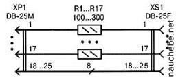
Fig. 4.8. The electrical circuit of the LPT cable with "anti-ring" resistors.
Connection schemes MK with LPT port can be divided into three groups:
Reception of signals from the computer (Fig. 4.9, a ... h);
Signal transmission to a computer (Fig. 4.10, a ... e);
Reception / transmission of signals at the same time (Fig. 4.11, a ... e).
The schemes adopted some simplifications. As the input signal, “DO” is mainly indicated, and “ASK” as the output signal, although there may be others listed in Table. 4.2. On each specific computer operability homemade circuits it is necessary to verify experimentally, which is associated with the presence of “strong” and “weak” LPT ports in terms of load capacity.
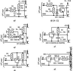
Fig. 4.9. Schemes for inputting signals from the LPT port to MK (start):
a) resistor R1 limits the input current. Elements R2, C1 may be absent, but they reduce “ringing” at the signal fronts with a long cable;
b) the buffer transistor VT1 inverts the signal. Diode VD1 is optional, but it protects the transistor from erroneously supplying a large negative voltage. If you do not install the resistor R2, then the circuit will remain operational, however, when the cable is undocked from the LPT port, the VT1 transistor may cause false positives from external interference and interference;
c) the diode VD1 cuts off the interference and increases the threshold of the transistor VT1. Resistor R1 reliably closes the transistor VT1 at a LOW level from the LPT port;
d) the buffer logic element DD1 has an open collector output. The signal fronts are formed by the elements R1, C1. You can put the K155LP9 repeater instead of the DD1 inverter, making the appropriate changes in the MK program and the computer;
d) Schmitt trigger DD1 (replacement - K555TL2) increases the noise immunity. The lower the resistance of the resistors R1, R2, the greater the steepness of the signal edges. When the cable from the LPT port is disconnected, the resistor R1 does not allow the input of the DD1 chip to "hang in the air";
f) the sequential inclusion of two logic elements DD11, /)/)/.2 increases (restores) the steepness of the signal edges. Resistor R1 eliminates emissions, "ringing";
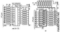
Fig. 4.9. Schemes for inputting signals from the LPT port to MK (end):
g) the data received from the LPT port is previously placed in the intermediate register DD1. Recording is performed at a HIGH level at the input “C” of the DD1 chip, and storage at LOW. This solution eliminates interference, because random data may be periodically displayed in the LPT port, depending on the drivers installed in the computer. They are eliminated programmatically, for example, by repeatedly reading the input signal from the MK lines;
h) buffering the LPT port with powerful transistor keys located in the Texas Instruments DA1 chip. Resistors R1 ... R8 can have 10 ... 15 times lower resistance, which allows you to connect in parallel to the outputs of the A4 chip / other components of the device.
Fig. 4.10. Schemes for outputting signals from MK to LPT port (start):
a) direct connection of MK output without buffer elements. Resistors R1, R2 reduce the reflection of signals in the line. In addition, the resistor R2 protects the MK output from accidental short circuit with the GND circuit in the wires of the connecting cable;
b) Schmitt trigger DD1 serves as a protective buffer for MK in case of emergency at the output (short circuit or high voltage supply);
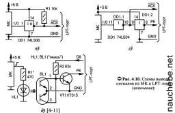
c) the DD1 chip has an open collector output, which protects it from a short circuit in the wires and connectors of the connecting cable;
d) the supply of two antiphase signals to the computer. Goal - software need or organization of a duplicate (control) data transmission channel;
d) opto-isolation on the elements HL1, BL1, which are used in computer mechanical "mice". The transistor KG / amplifies and inverts the signal. For normal operation of the device, the computer must set HIGH on the “D8” line.
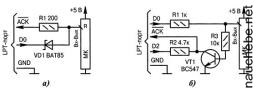
Fig. 4.11. Combined input / output signal circuits between MK and LPT port (start):
a) if the computer sets a “HIGH” level on the “DO” line, then MK in the output mode can generate an “ASK” signal through resistor R1. If MK is transferred to the input mode, the computer can transmit data to it via the “DO” line through the VD1 diode while the internal “pull-up” resistor MK forms a HIGH level;
b) the signal from the LPT port is input to MK through an inverter on the transistor VT1 and the computer should set HIGH on the line “D2”. Information in MK is entered from the DO line through resistor R1. The high resistance of resistor R1 physically decouples the input and output channels;
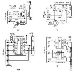
Fig. 4.11. Combined input / output signal circuits between MK and LPT port (end):
b) the signal from the LPT port is input to MK through the inverter on the transistor VT1, while the computer must set the LOW level on the line "DO". Information in MK is entered through the elements R1, R3, VT2;
d) the signal from the LPT port is input to MK through the repeater on the transistor VT1, while the computer should set HIGH on the line "DO". Information in MK is entered through the repeater on the DD1 chip \\
g) the signals "D0" ... "D3" are input to MK at a LOW level on the "INIT" line, and the computer must configure the lines "D4" ... "D7" as inputs. In the BIOS settings of the computer, you must set the bidirectional EPP or ECP mode for the LPT port. Information is transferred to the computer from the MK via the “D4” ... “D7” lines at a HIGH level on the “INIT” line. Resistor R1 transfers the outputs of the DD1 chip to the Z-state with the cable disconnected from the LPT port;
e) the signal from MK to the LPT port is entered through the repeater DD1.2, while the computer must set HIGH level on the line "D2" and LOW level on the line "D5". Information in MK is entered through the repeater DD1.1 at the LOW level of the line "D2". Gating signals at the inputs "E1", "E2" of the DD1 chip increases the reliability of data transmission.
Ministry of Education and Science of the Russian Federation
Federal State Budgetary Educational Institution
higher vocational education
"Komsomolsk-on-Amur State Technical University"
Department of Industrial Electronics
Testing the LPT port of a personal computer
Guidelines for laboratory work at the rate
"Debugging tools of microprocessor systems" for students of the direction 210100 "Electronics and nanoelectronics"
Komsomolsk-on-Amur 2013
Testing the LPT port of a personal computer: Methodological instructions for laboratory work on the course "Debugging means of microprocessor systems" for students in the direction 210100 "Electronics and Nanoelectronics" / Comp. CM. Hoofs. - Komsomolsk-on-Amur: Komsomolsk-on-Amur state. tech. Univ., 2013 .-- 19 p.
The Centronics parallel interface, signals and software support for the LPT port of a personal computer are considered, recommendations for its testing are given.
The proposed guidelines are intended for students in the direction 210100.
It is published by order of the editorial and publishing board of Komsomolsk-on-Amur State Technical University.
Agreed with the standardization department.
Reviewer V.A. Egorov
Objective: Explore the basic features of a standard LPT port. Master the principles of program-controlled information exchange through a parallel port. Learn to test its performance.
1 basic information
1.1 Description of the parallel interface
Historically, a parallel interface was introduced into a personal computer (PC) for connecting a printer (hence the abbreviation LPT - Line Printer - line printer). However, subsequently, a parallel interface began to be used to connect other peripheral devices (PU). The basic type of port allows you to transfer data in only one direction (from PC to PU), however, a number of bi-directional data transfer standards were later developed.
In modern office computers, an LPT port is usually not provided, however, by installing a multicard expansion port, you can get such a port at your disposal.
A parallel interface adapter is a set of registers located in the address space of I / O devices. The number of registers depends on the type of port, however, three of them are standard and are always present. This is a data register, a status register and a control register. Register addresses are counted from the base, the standard values \u200b\u200bof which are 3BCh, 378h, 278h. The port can use hardware interrupt (IRQ7 or IRQ9). Many modern systems allow you to change the port operating mode, its address and IRQ from the settings of the Base Input Output System (BIOS) Setup.
The LPT port has an external 8-bit data bus, a 5-bit status signal bus and a 4-bit control signal bus. Obviously, the port is asymmetric 12 lines work on output and only 5 on input.
At boot, the BIOS tries to detect a parallel port, and does it in a primitive and not always correct way a test byte consisting of an alternating set of zeros and ones (55h or AAh) is transmitted to the possible base addresses of the ports, then it is read at the same address, and if the read byte matches the recorded one, then it is considered that the LPT port is found at this address. Define Address lPT port4 BIOS cannot. To work with controllers in the BIOS, the INT 17h interrupt is provided, which provides the ability to transfer data (byte-by-bit), initialize the controllers and receive information about its status.
Centronics Conceptrefers to the signal set, communication protocol, and 36-pin connector previously installed in printers. The purpose of the signals and the contacts of the PU connector to which they are displayed are given in table 1.
Table 1 - Centronics Interface Signals
|
Direction |
Appointment |
|||
|
Data strobe. A computer is transmitted, data is recorded at a low signal level. |
||||
|
Data lines. D0 is the least significant bit. |
||||
|
Acknowledge - an acknowledgment pulse of a byte (request to receive the next one). It can be used to form an interrupt. |
||||
|
Busy. Data reception is only possible with a low signal level. |
||||
|
"1" indicates the end of the paper |
||||
|
"1" indicates the printer is turned on (GP - receiver readiness), usually +5 V through a resistor from the power source of the control panel) |
||||
|
Automatic line feed. If "0", then PU when receiving the character CR (carriage return) performs the function LF - line feed |
||||
|
PU error (off-line, no paper, no toner, internal error) |
||||
|
Initialization (go to the beginning of the line, reset all parameters to default values) |
||||
|
The choice of printer. When "1", the printer does not accept other interface signals |
||||
|
Common wire |
Note: column "T" - active signal level: "1" - high active level, "0" - low active level. The column "Direction" - the direction of transmission in relation to the printer: I - Input (input), O - Output (output).
The Auto LF signal is practically not used, but its incorrect value leads to the fact that the printer either skips lines, or prints lines on top of each other, or duplicates lines when printing in two passes.
The domestic analog of the Centronics interface is IRPR-M. In addition to it, there is an IRPI interface (outdated), which differs by the exchange protocol, the absence of an "Error" signal and the inversion of data lines. In addition, pairs of terminating resistors are connected to all input lines of the IRPR: 220 Ohms to +5 V and 330 Ohms to a common wire. This overloads most of the interface adapters of modern PCs.
The communication protocol for the Centronics interface is shown in Figure 1.
Figure 1 - Centronics Interface Communication Protocol
Transmission begins by checking the source of the Error signal. If it is installed, then the exchange is not made. Then the status of the Busy signal is checked. If it is "0", then the source proceeds to transmit the data byte. To transfer a byte, the source sets data bytes on the D0-D7 line and gives a signal Strobe #. The receiver by the signal Strobe # (hereinafter, the “#" sign after the signal name is a sign that the signal has a low active level) reads data from the data bus and sets the Busy signal for the duration of its processing. At the end of processing, the receiver generates an ACK # signal and removes the Busy signal.
If for a long time (6 - 12 sec) the source does not receive ACK #, then it makes a decision about the "time-out" error of the device. If after receiving the byte the receiver is for some reason not ready to receive data, then it does not remove the Busy signal. When programmatically implementing an exchange using the specified protocol, it is desirable to limit the waiting time for removing Busy (usually 30 - 45 seconds), otherwise the program may freeze.
The standard parallel port is called SPP (Standard Parallel Port). The SPP port is unidirectional, based on which the Centronics exchange protocol is implemented programmatically. The port provides IRQ generation by ACK # pulse at the input. Port signals are output to a standard DB-25S connector (socket), which is located directly on the adapter board or connected to it with a flat cable (in case the adapter is integrated with the motherboard).
The names of the signals correspond to the names of the Centronics interface signals (table 1), and the image of the interface adapter connector on the computer side is shown in Figure 2.
Table 2 - Connector and cable for standard LPT port
|
Loop wire | |||||||
|
10, 22, 14, 16, 18, 20, 22, 24, 26 |
Note. I / O - direction of transmission: I - input; O is the output; O (I) - output, the state of which can be read under certain conditions, O / I - output lines, the state of which is read when reading from the corresponding port registers. * - ACK # input is connected to +5 V power supply via 10 kOhm resistor. This is done to eliminate false interruptions, as the interrupt is generated by a negative signal drop at the input of ACK #.
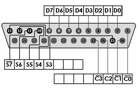
Figure 2 - Cetronics DB-25S Interface Adapter Connector
The disadvantages of the standard LPT port (SPP) are the low data transfer rate (100 - 150 kB / s), processor load during data transfer, and the impossibility of bidirectional byte exchange. There is a "amateur" bi-directional exchange technique, which consists in setting "1" to enter data on the D0-D7 line, and using open-collector microcircuits as a transmitter, which, when the transistor is open, can "raise" the logic unit voltage to the level about 1.5 - 1.7 V. Current is limited to 30 mA. As is obvious from the signal levels, they do not correspond to the TTL levels, so many ports do not work in this mode or work unstably. In addition, this method can be dangerous for the port adapter, which will work with current limits for it.
IEEE 1284 standardAdopted in 1994, defines the terms SPP, EPP and ECP. The standard defines 5 modes of data exchange, mode matching method, physical and electrical interfaces. According to IEEE 1284, the following communication modes are possible through the parallel port:
Compatibility Mode - Unidirectional (output) using the Centronics protocol. This mode corresponds to the standard SPP port;
Nibble Mode - enter a byte in two cycles (4 bits each), using to enter the status line. This exchange mode can be used on any adapter;
Byte Mode - input the entire byte, using to receive a data line. This mode only works on ports that allow reading of output data (Bi-Directional or PS / 2 Type 1);
EPP (Enhanced Parallel Port) Mode - bidirectional data exchange in which control signals of the interface are generated by hardware during a cycle of accessing the port (reading or writing to the port). Effective when working with external memory devices, LAN adapters;
ECP (Extended Capability Port) Mode - bidirectional exchange with the possibility of hardware data compression using the RLE (Run Length Encoding) method, the use of FIFO buffers and DMA. Interface control signals are generated by hardware. Effective for printers and scanners.
In modern machines with an LPT port on the system board, the port mode - SPP, EPP, ECP or a combination of them is set in the BIOS Setup. Compatibility Mode is fully compliant with SPP and is often set by default. All other modes expand the functionality of the interface and increase its performance. In addition, the standard regulates the method of negotiating the mode available for both a PC and a peripheral device.
Physical and electrical interface.The IEEE 1284 standard defines the physical characteristics of signal receivers and transmitters. It is essential that the transmission uses TTL levels of logic.
The IEEE 1284 standard defines three types of connectors used: A (DB-25S), B (Centronics-36), C (new small-sized 36-pin connector). Interface cables can have from 18 to 25 conductors (depending on the number of GND conductors). Conventional cables can only work at low speeds with a length of no more than 2 meters. Improved shielded cables with signal conductors interchanged with common wires can be up to 10 meters long. Such cables are marked as "IEEE Std 1284 - 1994 Compliant."
Low level parallel port operation (i.e., at the level of direct access to the port controller) is used when solving a different range of tasks for exchanging information with non-standard devices, for writing printer drivers and a number of other tasks. Direct work with the controller allows you to implement any communication protocol with the device and use the port lines as you wish.
The port controller is located in the address space of the input-output devices and it is accessed using the assembler IN and OUT commands. Information on LPT1 to LPT3 ports can be obtained by reading the BIOS variables shown in Table 3.
Table 3 - BIOS Variables for LPT Ports
|
Port name |
BIOS address |
Variable type |
Description |
|
The base address of the LPT1 port. If the variable is 0, then port LPT1 was not found |
|||
|
Timeout Constant |
|||
|
The base address of the LPT2 port. If the variable is 0, then LPT2 port is not found |
|||
|
Timeout Constant |
|||
|
The base address of the LPT3 port. If the variable is 0, then LPT3 port is not found |
|||
|
Timeout Constant |
|||
|
The base address of the LPT4 port. If the variable is 0, then LPT4 port is not found |
|||
|
Timeout Constant |
The BIOS looks for ports at Base addresses: 3BCh, 378h, 278h. LPT4 BIOS port cannot be found:
378h - parallel adapter LPT1;
278h - parallel adapter LPT2;
3BCh - LPT3 parallel adapter.
The standard port has three 8-bit registers located at neighboring addresses, starting with the base address. The list of these registers is given in table 4.
Table 4 - Registers of the standard LPT port
Data Register (DR).The data recorded in this register is output to the output lines of the D0D7 interface. The result of reading this register depends on the adapter circuitry and corresponds to either the previously recorded data or the signals on the D0D7 lines, which is not always the same. With standard inclusion, the first option is valid - the read data is equal to the previously recorded.
Status Register (SR). It is a 5-bit input port to which status signals from an external device are connected. Allows read only. The bit assignment of this register is shown in table 5.
Table 5 - SR Status Register Bits
|
Title |
Appointment |
|
|
Inverse display of Busy line status (11). At a low level on line 11 (Busy) - the bit is "1" - the control panel is ready to receive the next byte |
||
|
Displays the status of the ACK # line (10). "0" - confirmation of receipt, "1" - normal state |
||
|
Displays the status of the Paper End line (12). "0" is the norm, "1" is no paper in the control panel |
||
|
Displays the status of the Select line (13). "0" - no PU selected, "1" - no PU selected |
||
|
(inverse) |
Error line status display (15). "0" - PU error, "1" - normal state |
|
|
ACK # interrupt flag (PS / 2 only). Zero if ACK # caused a hardware interrupt. "1" - after reset or after reading the status register |
||
|
Not used (reserve) |
Management Register (CR).The control register is a 4-bit output port that allows reading and writing. Bits 0, 1, 3 are inverted, i.e. "1" in these bits of the control register corresponds to "0" on the corresponding port lines. The control register bits are shown in Table 6. Bit 5 is used only by bidirectional ports.
Table 6 - CR Management Register Bits
|
Title |
Appointment |
|
|
Port Direction Control Bit. "1" - input mode, "0" - output mode |
||
|
ACK # Interrupt Generation Control Bit. "1" - enable ACK # recession interruption (10) |
||
|
Line control SLCT IN # (17). "1" - the printer is enabled. |
||
|
Controlling the INIT # line (16). "1" - normal state, "0" - hardware reset of the control panel |
||
|
Auto LF # line control (14). "1" - enable "Auto LF" mode, "0" - normal state |
||
|
Control line Strobe # (1). "1" - gating data, "0" - normal state |
Interface programming. To develop application programs, you must select a programming language. If you need a simple, fast and compact program that does not contain complex computational operations, then for writing it it is better to choose a low-level language (assembly language). Assembly language belongs to the group of machine-oriented languages, i.e. each microprocessor family has its own language.
Tongue high level you should choose if you need to perform complex calculations, or if high-speed program is not required. Object codes obtained as a result of translating programs written in a high-level language usually take up much more space in the computer's memory and execute more slowly compared to assembler programs. An approach is often used when parts of a program critical to speed are written in assembler, and computational procedures are written in a high-level language, for example, Pascal or C.
Consider working with registers of the CENTRONICS interface in PASCAL or assembler:
X is a number of type "byte" (0..255). For example, when sending 170 10 \u003d \u003d 10101010 2 on the line d0 – d7, a single signal will be present on the terminals d1, d3, d5, d7 (the designation of the terminals starts with d0). The number 170 will remain on the pins of the connector until you send another number there (another program can do this) or turn off the computer. Note that the port address in the command is specified in hexadecimal, and the package in decimal. If instead of the Pascal command
Port [$ 378]: \u003d 170;
You apply
where d is a variable, the variable will take the value of the last byte sent to the port or, when switching to receive mode, the value of the byte sent to the port by an external device.
An example of reading the status register in Pascal:
In the variable d, after the program is executed, the port status will be displayed. Let's say the variable returned the value 126 10. In binary form, it looks like 01111110 2. The lower (right) three bits (zero, first and second) are not used, and are almost equal to 1, 1 and 0. The third bit is 1, which means that ERROR is at a high level. The situation is the same on SELECT, Paper End, ACK and BUSY (do not forget that the BUSY signal is inverted).
Here is an example of a fragment of a program that reads bytes from data lines D0-D7:
Port [$ 37A]: \u003d 32; a value of 32 "includes" a unit in the fifth
d: \u003d Port [$ 378]; beat by putting the port in input mode
As can be seen from the above examples, programming the LPT port is a very simple task, which can greatly facilitate the work of the software developer of the devices with the discussed interface.
1.2 Testing the LPT port
Testing the LPT port can be done using a simple stub, which can be made using table 7.
Table 7 - Table of the stub circuits for testing the LPT port
|
Direction |
Direction | ||||
Parallel Port and RPR
Most of the modern peripherals connected to the LPT-nop support 1284 standard and Rpr functions. To support these functions, a computer, from a hardware point of view, is enough to have an interface controller that conforms to the 1284 standard. If the connected device supports RPR, it can “negotiate” with the port representing the “interests” of the computer about possible exchange modes using the mode matching protocol 1284. Further, for the RPR to work, the connected device must inform the operating system of all the necessary information about itself. At a minimum, these are manufacturer identifiers, models, and a set of supported commands. More detailed device information may include a class identifier, detailed description and the identifier of the device with which it is compatible. In accordance with the accepted information to support this device operating system may take steps to install the required software.
Devices with RPR support are recognized by the OS at the stage of its loading, unless, of course, they are connected to the port by an interface cable and they have power on. If Windows discovers a connected Rpr device that differs from what is written in its registry for this port (or just a new device), it tries to install the drivers required for the device from the OS distribution kit or from the package supplied with the new device. If Windows does not want to notice a newly connected PPR device, this may indicate a port or cable malfunction. The RPR system does not work if the device is connected with a cheap “non-bidirectional” cable that has no Selectln # connection (pin 17 of the LPT port and pin 36 of the Centronics connector).
Typically, the LPT port is used to connect the printer (see clause 8.3.1), however, this does not cover its use.
To connect two computersvarious cables are used on the parallel interface depending on the modes of the ports used. The easiest and slowest - nibble mode running on allports. For this mode, it is enough to have 10 signal and one common wire in the cable. The wiring of the cable connectors is given in table. 1.11. The connection of two PCs with this cable is supported by standard software such as Interlnk from MS-DOS or Norton Commander.
High-speed communication between two computers can also be performed in the ECP mode (the EPP mode is inconvenient because it requires synchronization of the input / output bus cycles of two computers).
Connection scannerto an LPT port is effective only if the port provides at least bi-directional mode (Bi-Di),since the main thread is input. It is better to use the ECP port if this mode is supported by the scanner (or EPP, which is unlikely).
Connection external drives(Iomega Zip Drive, CD-ROM, etc.), lAN adaptersand other symmetrical input-output devices has its own specifics. In SPP mode, along with the slowdown of the device, a fundamental asymmetry of this mode is noticeable: reading datagoing on twice slower than(very slow) record.Application bidirectionalregime (Bi-Dior PS / 2 Tour 1)eliminate this asymmetry - speeds will equal.Only by switching to EPP or ESR, you can get normalspeed of work. In the EPP or ECP mode, the connection to the LPT port is almost as fast as the connection through the ISA controller. This is also true when connecting devices with a standard bus interface to LPT ports through interface converters (for example, LPT - IDE, LPT - SCSI, LPT - PCMCIA). Note that the IDE hard drive connected via an adapter to the LPT port can be represented as a SCSI device for the system (this is more logical from a software point of view).
2. Serial Interfaces
The serial interface for data transmission uses a single signal line along which information bits are transmitted one after another in series. Hence the name of the interface and port. English terms - Serial interface and Serial part (sometimes they are incorrectly translated as "serial"). Serial transmission reduces the number of signal lines and increases the communication range. A characteristic feature is the use of non-TTL signals. A number of serial interfaces use galvanic isolation of external (usually input) signals from the circuit ground of the device, which allows connecting devices under different potentials. Below we will consider the interfaces RS-232C, RS-422A, RS-423A, RS-485, current loop, MIDI, as well as the COM port.
2.1. Serial Transmission Methods
Serial data transfer can be carried out in asynchronous or synchronous modes. At asynchronous each byte is preceded by start bit signaling to the receiver of the start of the package, followed by data bits and, perhaps, parity bit (parity). Completes the package stop bit guaranteeing a pause between parcels (Fig. 2.1). The start bit of the next byte is sent at any time after the stop bit, that is, pauses of arbitrary duration are possible between transmissions. The start bit, which always has a strictly defined value (logical 0), provides a simple mechanism for synchronizing the receiver according to the signal from the transmitter. It is understood that the receiver and transmitter operate at the same exchange rate. The receiver’s internal clock generator uses a reference frequency divider counter that is reset to zero at the time the start bit is received. This counter generates internal gates by which the receiver captures subsequent received
bits. Ideally, the gates are located in the middle of the bit intervals, which allows data to be received even with a slight mismatch between the receiver and transmitter speeds. Obviously, when transferring 8 data bits, one control and one stop bit, the maximum permissible speed mismatch, at which the data will be recognized correctly, cannot exceed 5%. Taking into account phase distortions and discrete operation of the internal synchronization counter, a lower frequency deviation is actually permissible. The lower the division ratio of the reference frequency of the internal oscillator (the higher the transmission frequency), the greater the error in the binding of the gates to the middle of the bit interval, and the requirements for frequency matching become more stringent. The higher the transmission frequency, the greater the influence of edge distortions on the phase of the received signal. The interaction of these factors leads to increased requirements for the consistency of the frequencies of the receiver and transmitter with an increase in the exchange frequency.
The asynchronous send format allows you to identify possible transmission errors:
» If a difference is received that signals the beginning of the sending, and the logical unit level is fixed at the start-bit strobe, the start-bit is considered false and the receiver switches back to the standby state. The receiver may not report this error.
“If during the time allotted for the stop bit, a logic zero level is detected, a stop bit error is recorded.
"« If parity is applied, then after sending the data bit is transmitted control bit. This bit complements the number of unit data bits to even or odd, depending on the accepted agreement. Receiving a byte with an invalid control bit value will fix the error.
Format control allows detecting a line break:
in this case, a logical zero is accepted, which is first treated as a start bit, and zero data bits, then the stop bit control is triggered.
A series is accepted for asynchronous mode standard exchange rates: 50, 75, 110, 150,300,600,1200,2400,4800,9600, 19 200, 38 400, 57 600 and 115 200 bit / s. Sometimes, instead of a “bps” unit of measurement, a “baud” is used, but when considering binary transmitted signals, this is incorrect. In bauds, it is customary to measure the frequency of a line state change, and with a non-binary coding method (widely used in modern modems) in a communication channel, bit rates (bps) and signal changes (baud) can differ several times (for details, see Appendix A )
number data bit can be 5, 6, 7 or 8 (5- and 6-bit formats are not widely distributed). Quantity stop bit it can be 1, 1,5 or 2 (“one and a half bit” means only the length of the stop interval).
Asynchronous exchange in PC implemented using COM port with using protocol RS-232C.
Synchronous transmission mode assumes constant activity of the communication channel. Sending begins with a sync byte, immediately followed by a stream of information bits. If the transmitter does not have data to transmit, it fills the pause by continuously sending synchronization bytes. Obviously, when transferring large amounts of data, the overhead for synchronization in this mode will be lower than in asynchronous. However, in synchronous mode, external synchronization of the receiver with the transmitter is necessary, since even a small frequency deviation will lead to distortion of the received data. External synchronization is possible either using a separate line for transmitting the synchronization signal, or using self-synchronizing data encoding, in which synchronization pulses can be extracted from the received signal from the received signal. In any case, synchronous mode requires expensive communication lines or terminal equipment. For PC, there are special boards - SDLC adapters (expensive) that support synchronous exchange mode. They are used mainly for communication with large IBM machines (mainframes) and are not widely used. Of synchronous adapters, V.35 interface adapters are currently used.
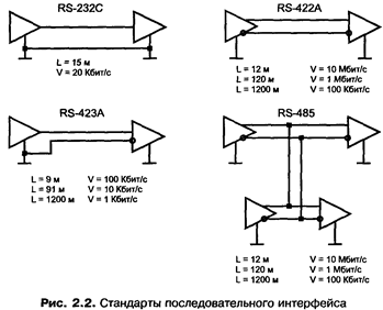
On physical level the serial interface has various implementations that differ in the way electrical signals are transmitted. There are a number of related international standards: RS-232C, RS-423A, RS-422A and RS-485. In fig. Figure 2.2 shows the connection diagrams of the receivers and transmitters, and also shows the restrictions on the line length (L) and the maximum data rate (V).
Unbalanced interface lines RS-232C and RS-423Ahave the lowest common mode immunity, although the receiver differential input RS-423A softens the situation somewhat. Top options has a point-to-point interface RS-422A and its trunk (bus) analog RS-485, working on symmetrical communication lines. They use differential signals with a separate (twisted) pair of wires to transmit each signal.
In the listed standards, the signal appears potential. There are serial interfaces, where the current flowing through the common transmitter-receiver circuit is “current loop” and MIDI. For short-distance communications, wireless infrared standards have been adopted. The most widely used in PCs was the simplest of these - the standard RS-232Cimplemented by COM ports. In industrial automation is widely used RS-485, and RS-422A, found in some printers. Signal converters exist for matching these related interfaces.
2.2. RS-232C interface
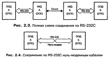
The interface is designed to connect equipment transmitting or receiving data (OOD - data terminal equipment or ADF - data transmission equipment; DTE - Data Terminal Equipment), to data channel terminal equipment (AKD; DCE - Data Communication Equipment). The ADF can be a computer, printer, plotter, and other peripheral equipment. The role of AKD is usually a modem. The ultimate goal of connecting is to connect two ADF devices. A complete connection diagram is shown in Fig. 2.3. The interface allows you to exclude a remote communication channel together with a pair of ADF devices by connecting devices directly using a null modem cable (Fig. 2.4).
The standard describes interface control signals, data transfer, electrical interface and connector types. The standard provides for asynchronous and synchronous exchange modes, but COM ports only support asynchronous mode. Functionally RS-232C equivalent to CCITT V.24 / V.28 and C2, but they have different signal names.
2.2.1. Electrical interface
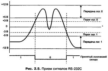
Standard RS-232C uses asymmetric transmitters and receivers - the signal is transmitted relative to the common wire - the circuit ground (symmetrical differential signals are used in other interfaces - for example, RS-422). Interface DOES NOT PROVIDE ELECTRICAL DISCONNECTION devices. Logical unit corresponds to voltage on receiver input in the range of -12 ...- 3 V. For control signal lines, this state is called ON (“On”), for serial data lines - MARK. The logical range of +3 ... + 12 V corresponds to logical zero. For control signal lines, the state is called Off (“Off”), and for serial data lines - SPACE The range of -3 ... + 3 V is the dead band, which determines the hysteresis of the receiver: the state of the line will be considered changed only after crossing the threshold (Fig. 2.5). The signal levels at the outputs of the transmitters should be in the ranges -12 ...- 5 V and +5 ... + 12 V to represent unity and zero, respectively. The potential difference between the circuit earths (SG) of the connected devices must be less than 2 V, with a higher potential difference, incorrect signal perception is possible. Interface assumes availability PROTECTIVE EARTHING for connected devices, if both of them are powered by AC power and have line filters.
Connect and disconnect interface cables self-powered devices should be produced when the power is off. Otherwise, the difference in the unbalanced potentials of the devices at the time of switching may turn out to be applied to the output or input (which is more dangerous) interface circuits and damage the microcircuit.
For interface RS-232C specially prepared buffer receiver microcircuits (with hysteresis and a bipolar signal transmitter). If grounding and switching rules are not followed, they are usually the first victims of pyrotechnic effects. Sometimes they are installed in "beds", which facilitates the replacement. Signal Conditioning Chip Pinout RS-232C shown in fig. 2.6. Often, buffer circuits are included directly in the interface LSI. This reduces the cost of the product, saves space on the board, but in the event of an accident turns into large financial losses. It is unlikely to disable interface microcircuits by shorting the signal circuits: the short-circuit current of the transmitters usually does not exceed 20 mA. 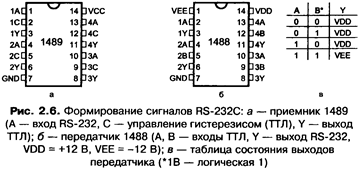
Standard RS-232C governs types of connectors used.
On equipment ADF (including on COM ports) it is customary to install forks (male - "dad") DB-25P or more compact option - DB-9P. Nine-pin connectors do not have contacts for additional signals necessary for synchronous operation (in most 25-pin connectors, these contacts are not used).
On equipment AKD (modems) install sockets(female - “mother”) DB-25Swm DB-9S.
This rule assumes that the connectors AKD can connect to connectors ADF directly or through transitional “direct” cables with a socket and a plug, in which the contacts are connected “one to one”. Adapter cables can also be adapters with 9- to 25-pin connectors (Fig. 2.7).
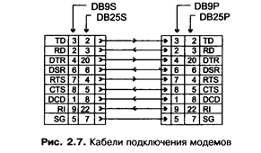
If the equipment ADF is connected without modems, then the device connectors (plugs) are interconnected null modem cable (Zero-modem or Z-modem), which has sockets at both ends, the contacts of which are connected crosswise according to one of the circuits shown in Fig. 2.8.

If on any device ADF a socket is installed - this is an almost absolute sign that it should be connected to another device with a direct cable, similar to a modem cable. The outlet is usually installed on those devices for which remote connection via modem is not provided.
In the table. 2.1 shows the purpose of the contacts of the connectors of the COM ports (and any other equipment ADF). The DB-25S connector pins are defined by the EIA / TIA-232-E standard, the DB-9S connector is described by the EIA / TIA-574 standard. For modems, the name of the circuits and contacts is the same, but the roles of the signals (input-output) are reversed.
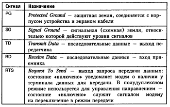
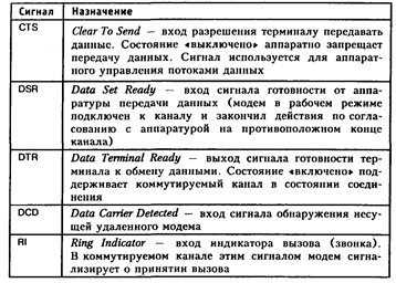
Subset of signals RS-232C related to asynchronous mode, we consider from the point of view of the COM port of the PC. It should be remembered that the active state of the signal (“on”) and logical unit transmitted data corresponds negative potential (below -3 V) of the interface signal, and the state is “off” and logical zero - positive (above +3 V). The purpose of the interface signals is given in table. 2.2. 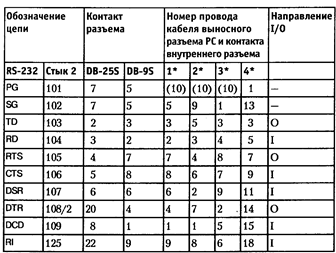
1 * - a loop of 8-bit multicards.
2 * - a loop of 16-bit multicards and ports on motherboards. 3 * - a variant of a port loop on motherboards. 4 * - a wide loop to the 25-pin connector.
2.2.2. Data flow control
To control the flow of data (Flow Control), two protocol options can be used - hardware and software. Sometimes flow control is confused with acknowledgment, but these are different methods for achieving one goal - coordinating the rate of transmission and reception. Acknowledgment(Handshaking) means sending a notification about the receipt of the item, while flow control involves sending a notification of the impossibility of subsequent reception of data.
Hardware Flow Control Protocol RTS / CTS (Hardware Flow Control) uses the CTS signal, which allows you to stop data transfer if the receiver is not ready to receive them (Fig. 2.9). The transmitter "releases" the next byte only when the CTS line is on. A byte that has already begun to be transmitted cannot be delayed by the CTS signal (this guarantees the integrity of the sending). The hardware protocol provides the fastest response of the transmitter to the state of the receiver. Asynchronous transceiver microcircuits have at least two registers in the receiving part -
shifting, for receiving the next sending, and storing, from which the received byte is read. This allows the exchange of hardware protocol without data loss.
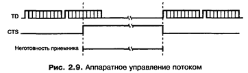
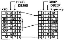
The hardware protocol is convenient to use when connecting printers and plotters, if they support it (Fig. 2.10). For direct (without modems) connecting two computers, the hardware protocol requires cross-connection of RTS - CTS lines.
If the hardware protocol is not used, the transmitting terminal must have an “on” state on the CTS line with the RTS-CTS jumper. Otherwise, the transmitter will be silent.
XON / XOFF flow control software protocol assumes a bi-directional data channel. The protocol works as follows: if the device receiving the data detects the reasons for which it can no longer receive it, it sends a byte character on the reverse serial channel Xoff (13h). The opposite device, having accepted this symbol, pauses transmission. When the receiving device again becomes ready to receive data, it sends a character
Xon (llh) by accepting which the opposite device resumes transmission. The response time of the transmitter to a change in the state of the receiver compared with the hardware protocol is increased at least by the time the symbol is transmitted (XON or XOFF) plus the response time of the transmitter program to receive a character (Fig. 2.11). It follows that lossless data can only be received by a receiver having an additional buffer of received data and signaling unavailability in advance (having free space in the buffer).
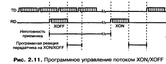
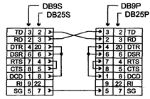
The advantage of the software protocol is that there is no need to transmit interface control signals - the minimum cable for two-way exchange can have only 3 wires (see Fig. 2.8a). The disadvantage, in addition to requiring a buffer and a longer reaction time (which reduces the overall performance of the channel due to signal waiting XON) is the difficulty of implementing a full duplex exchange mode. In this case, flow control symbols should be extracted (and processed) from the received data stream, which limits the set of transmitted symbols. Minimum cable option for connecting a printer (plotter) with protocol XON / XOFF shown in fig. 2.12.
In addition to these two common standard protocols supported by both PU and OS, there are others. Some serial plotters use software control, but send non-standard characters XON / XOFF, but the words (ASCII lines). Such an exchange is practically not supported at the level of system support for the protocol (these plotters directly "talk" with the application program). Of course, you can write a COM port driver (interceptor INT 14h) but the need to process text messages from the output device in it usually does not delight the system programmer. The cable for connection matches the one shown in fig. 2.12.
2.3. Current Loop Interface
A common option for a serial interface is a current loop. In it, the electric signal is not the voltage level relative to the common wire, but current in a two-wire line connecting the receiver and transmitter. A logical unit (“on” state) corresponds to a current flow of 20 mA, and a logical zero corresponds to a lack of current. Such a representation of signals for the described format of asynchronous sending allows detecting a line break - the receiver will notice the absence of a stop bit (line break acts as a constant logical zero).
The current loop usually assumes galvanic isolation input circuits of the receiver from the device circuit. The current source in the loop is the transmitter (this option is called the active transmitter). It is also possible to receive power from the receiver (active receiver), while the transmitter output key can also be galvanically isolated from the rest of the transmitter circuit. Simplified options exist without galvanic isolation, but this is already a degenerate case of the interface. The galvanically isolated current loop allows signals to be transmitted over distances of up to several kilometers. The distance is determined by the resistance of the pair of wires and the level of interference. Since the interface requires a pair of wires for each signal, usually only two interface signals are used. In the case of bidirectional exchange, only the signals of the transmitted and received data are used, and the program method is used to control the flow XON / XOFF. If bidirectional exchange is not required, use one data line, and to control the flow, the return line is used for the CTS signal (hardware protocol) or oncoming data line (software protocol).
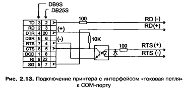
Convert signals RS-232C into the current loop is possible using a simple circuit (Fig. 2.13). Here the printer is connected via a current loop to the COM port with hardware flow control. To obtain the bipolar signal required for the input signals of the COM port, power is applied from the interface.
With proper software, a single current loop can provide bi-directional half-duplex communication between two devices. In this case, each receiver “hears” both the signals of the transmitter on the opposite side of the channel, and the signals of its transmitter. They are regarded by communication packets simply as an echo. For error-free reception, the transmitters must operate alternately.
2.4. MIDI Interface
Digital interface musical instruments MIDI(Musical Instrument Digital Interface) is a bidirectional serial asynchronous interface with a transmission frequency of 31.25 Kbps. This interface, developed in 1983, has become the de facto standard for interfacing computers, synthesizers, recording and reproducing devices, mixers, special effects devices, and other electro-musical equipment.
The interface applies such a loop 10 mA (maybe 5 mA) with galvanic isolation of the input circuit. This eliminates the connection of "circuit lands" of the connected devices via an interface cable, eliminating interference that is extremely undesirable for sound equipment. The interference frequency is also reduced by the choice of the transmission frequency, which coincides with one of the values \u200b\u200bof the quantization frequencies adopted in digital sound recording.
Asynchronous package contains a start bit, 8 bits of information and 1 stop bit, there is no parity. The high bit of the send is a command / data indication. Its zero value indicates the presence of seven data bits in the least significant bits. At a single value, the bits contain team code and the bits are channel number. Commands can be either addressed to a specific channel or broadcast addressless. The last group includes start, stop, and timestamps that synchronize devices (synchronization system MIDI Sync and MTS - MIDI Time Code).
An interface defines three types of ports: MIDI-In, MIDI-Out nMIDI-Thru.
MIDI-In Input Port represents the input of the “10 mA current loop” interface, galvanically isolated from the receiver by an optocoupler with a speed of at least 2 μs. The device monitors the information flow at this input and responds to commands and data addressed to it.
MIDI Out Port represents the output of a 10 mA current source galvanically coupled to a device circuit. The limiting resistors protect the output circuits from damage when shorted to ground or a 5 V source. An information stream from this device is supplied to the output. The stream may contain a translated input stream.
MIDI Thru Transit Port (optional) serves to relay the input signal.
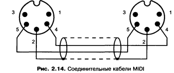
As connectors, 5-pin DIN connectors are used, which are common in household audio equipment. Sockets are installed on all devices, and plugs are installed on the cables. All MIDI connecting cables are unified (Fig. 2.14). Pin 2 - cable shield - connects to the common wire only on the transmitter side (on the connectors MIDI Out and MIDI-Thru).
In the labeling of the inputs and outputs indicated near the connectors, there are different interpretations. Some manufacturers write “In” or “Out” in accordance with the connector function of this device (and this is correct), then any cable connects “In” and “Out”. Others believe that the signature should indicate the function of the connected device. Then the cable will connect the connectors with the designations “In” - “In” and “Out” - “Out”.
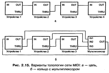
The interface allows you to combine a group of up to 16 devices in local network. The topology must obey the rule:
input MIDI In one device must be connected to the output MIDI Out or MIDI Thru of another. When planning a MIDI network, you must be guided by information flows and device communications. Control devices - keyboards, sequencers (in playback mode), synchronization sources - must be in front of the controlled ones. If devices need bidirectional exchange, they are connected in a ring. It is possible to use special multiplexers that allow you to logically switch multiple input streams into one output. A degenerate case of a ring is a bi-directional connection of two devices. Several connection options are shown in Fig. 2.15.
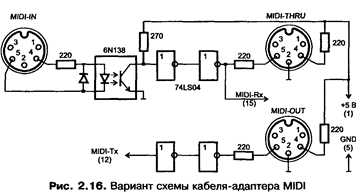
The PC has a MIDI port on most audio adapters; its signals are output to the unused pins (12 and 15) of the game adapter connector. Connecting MIDI devices requires adapter adapter implements the interface "current loop". The adapter adapter is usually built into a special cable, the circuit of which is shown in Fig. 2.16. Some PC models have built-in adapters and standard 5-pin MIDI connectors.
The PC uses MIDI-compatible ports for the controller MPU-401 (Roland) in UART mode. In the input / output space MPU-401 occupies two adjacent addresses MPU (usually 330h) and MPU + 1:
"» Port DATA (address MPU + 0) - writing and reading bytes transmitted and received via the MIDI interface. Port STATUS / COMMAND (address MPU + 1) - read status / write commands (write - only for intelligent mode). The following bits are defined in the status byte:
Bit 7 - DSR (Data Set Ready) - availability (DSR-0) received data to read. The bit is set to “I” when all received bytes are read from the data register.
Bit 6 - DRR (Data Read Ready) - readiness (DRR \u003d 0)UART to write to the data register or commands. The condition of readiness for writing does not occur if the receiver has an unread byte of data.
Some motherboards use LSI interface controllers in which the UART used for the COM port can be set to the MIDI port mode by configuring via BIOS.