Radio components - symbols on the diagram. How to read the designations of radio components on the diagram? Secrets of foreign radio circuits Designation on diagram c
Beginning radio amateurs are often faced with the problem of identifying radio components on diagrams and correctly reading their markings. The main difficulty lies in the large number of names of elements, which are represented by transistors, resistors, capacitors, diodes and other parts. Its practical implementation and normal operation of the finished product largely depend on how correctly the diagram is read.
Resistors
Resistors include radio components that have a strictly defined resistance to the electric current flowing through them. This function is designed to reduce the current in the circuit. For example, to make a lamp shine less brightly, power is supplied to it through a resistor. The higher the resistance of the resistor, the less the lamp will glow. For fixed resistors, the resistance remains unchanged, while variable resistors can change their resistance from zero to the maximum possible value.
Each constant resistor has two main parameters - power and resistance. The power value is indicated on the diagram not with alphabetic or numerical symbols, but with the help of special lines. The power itself is determined by the formula: P = U x I, that is, equal to the product of voltage and current. This parameter is important because a particular resistor can only withstand a certain amount of power. If this value is exceeded, the element will simply burn out, since heat is released during the passage of current through the resistance. Therefore, in the figure, each line marked on the resistor corresponds to a certain power.

There are other ways to designate resistors in diagrams:

- On the circuit diagrams, the serial number is indicated in accordance with the location (R1) and the resistance value is equal to 12K. The letter “K” is a multiple prefix and means 1000. That is, 12K corresponds to 12,000 ohms or 12 kilo-ohms. If the letter “M” is present in the marking, this indicates 12,000,000 ohms or 12 megaohms.
- In marking with letters and numbers, the letter symbols E, K and M correspond to certain multiple prefixes. So the letter E = 1, K = 1000, M = 1000000. The decoding of the symbols will look like this: 15E - 15 Ohm; K15 - 0.15 Ohm - 150 Ohm; 1K5 - 1.5 kOhm; 15K - 15 kOhm; M15 - 0.15M - 150 kOhm; 1M2 - 1.5 mOhm; 15M - 15mOhm.
- In this case, only digital designations are used. Each includes three digits. The first two of them correspond to the value, and the third - to the multiplier. Thus, the factors are: 0, 1, 2, 3 and 4. They indicate the number of zeros added to the base value. For example, 150 - 15 Ohm; 151 - 150 Ohm; 152 - 1500 Ohm; 153 - 15000 Ohm; 154 - 120000 Ohm.
Fixed resistors
The name of constant resistors is associated with their nominal resistance, which remains unchanged throughout the entire period of operation. They differ depending on the design and materials.

Wire elements consist of metal wires. In some cases, high resistivity alloys may be used. The basis for winding the wire is a ceramic frame. These resistors have high nominal accuracy, but a serious drawback is the presence of a large self-inductance. In the manufacture of film metal resistors, a metal with high resistivity is sprayed onto a ceramic base. Due to their qualities, such elements are most widely used.
The design of carbon fixed resistors can be film or volumetric. In this case, the qualities of graphite as a material with high resistivity are used. There are other resistors, for example, integral ones. They are used in specific integrated circuits where the use of other elements is not possible.
Variable resistors
Beginning radio amateurs often confuse a variable resistor with a variable capacitor, since in appearance they are very similar to each other. However, they have completely different functions, and there are also significant differences in how they are represented on the circuit diagrams.

The design of a variable resistor includes a slider that rotates along the resistive surface. Its main function is to adjust the parameters, which consists in changing the internal resistance to the desired value. The operation of the volume control in audio equipment and other similar devices is based on this principle. All adjustments are made by smoothly changing voltage and current in electronic devices.
The main parameter of a variable resistor is its resistance, which can vary within certain limits. In addition, it has an installed power that it must withstand. All types of resistors have these qualities.

On domestic circuit diagrams, elements of variable type are indicated in the form of a rectangle, on which two main and one additional terminal are marked, located vertically or passing through the icon diagonally.
In foreign diagrams, the rectangle is replaced by a curved line indicating an additional output. Next to the designation is the English letter R with the serial number of a particular element. The value of the nominal resistance is indicated next to it.
Connection of resistors
In electronics and electrical engineering, resistor connections are often used in various combinations and configurations. For greater clarity, you should consider a separate section of the circuit with serial, parallel and.

In a series connection, the end of one resistor is connected to the beginning of the next element. Thus, all resistors are connected one after another, and a total current of the same value flows through them. Between the start and end points there is only one path for current to flow. As the number of resistors connected into a common circuit increases, there is a corresponding increase in the total resistance.

A connection is considered parallel when the starting ends of all resistors are combined at one point, and the final outputs at another point. Current flow occurs through each individual resistor. As a result of parallel connection, as the number of connected resistors increases, the number of paths for current flow also increases. The total resistance in such a section decreases in proportion to the number of connected resistors. It will always be less than the resistance of any resistor connected in parallel.

Most often in radio electronics, a mixed connection is used, which is a combination of parallel and serial options.
In the diagram shown, resistors R2 and R3 are connected in parallel. The series connection includes resistor R1, a combination of R2 and R3, and resistor R4. In order to calculate the resistance of such a connection, the entire circuit is divided into several simple sections. After this, the resistance values are summed up and the overall result is obtained.
Semiconductors
A standard semiconductor diode consists of two terminals and one rectifying electrical junction. All elements of the system are combined in a common housing made of ceramic, glass, metal or plastic. One part of the crystal is called the emitter, due to the high concentration of impurities, and the other part, with a low concentration, is called the base. The marking of semiconductors on the diagrams reflects their design features and technical characteristics.

Germanium or silicon is used to make semiconductors. In the first case, it is possible to achieve a higher transmission coefficient. Elements made of germanium are characterized by increased conductivity, for which even a low voltage is sufficient.
Depending on the design, semiconductors can be point or planar, and according to technological characteristics they can be rectifier, pulse or universal.
Capacitors
A capacitor is a system that includes two or more electrodes made in the form of plates - plates. They are separated by a dielectric, which is much thinner than the capacitor plates. The entire device has mutual capacitance and has the ability to store electrical charge. In the simplest diagram, the capacitor is presented in the form of two parallel metal plates separated by some kind of dielectric material.

On the circuit diagram, next to the image of the capacitor, its nominal capacitance is indicated in microfarads (μF) or picofarads (pF). When designating electrolytic and high-voltage capacitors, after the rated capacitance the value of the maximum operating voltage, measured in volts (V) or kilovolts (kV), is indicated.
Variable capacitors
To designate capacitors with variable capacitance, two parallel segments are used, which are crossed by an inclined arrow. Movable plates connected at a certain point in the circuit are depicted as a short arc. Next to it is a designation for the minimum and maximum capacity. A block of capacitors, consisting of several sections, is combined using a dashed line intersecting the adjustment signs (arrows).

The trimmer capacitor designation includes a slanted line with a dash at the end instead of an arrow. The rotor appears as a short arc. Other elements - thermal capacitors - are designated by the letters SK. In its graphic representation, a temperature symbol is placed next to the nonlinear regulation sign.
Permanent capacitors
Graphic symbols for capacitors with constant capacitance are widely used. They are depicted as two parallel segments and conclusions from the middle of each of them. The letter C is placed next to the icon, after it - the serial number of the element and, with a small interval, a numerical designation of the nominal capacity.


When using a capacitor with in a circuit, an asterisk is placed instead of its serial number. The rated voltage value is indicated only for high voltage circuits. This applies to all capacitors except electrolytic ones. The digital voltage symbol is placed after the capacity designation.
The connection of many electrolytic capacitors requires correct polarity. In the diagrams, a “+” sign or a narrow rectangle is used to indicate a positive cover. In the absence of polarity, narrow rectangles mark both plates.
Diodes and Zener diodes
Diodes are the simplest semiconductor devices that operate on the basis of an electron-hole junction known as a pn junction. The property of one-way conductivity is clearly conveyed in graphic symbols. A standard diode is depicted as a triangle, symbolizing the anode. The apex of the triangle indicates the direction of conduction and abuts the transverse line indicating the cathode. The entire image is intersected in the center by an electrical circuit line.

The letter designation VD is used. It displays not only individual elements, but also entire groups, for example, . The type of a particular diode is indicated next to its position designation.
The basic symbol is also used to designate zener diodes, which are semiconductor diodes with special properties. The cathode has a short stroke directed towards the triangle, symbolizing the anode. This stroke is positioned unchanged, regardless of the position of the zener diode icon on the circuit diagram.
Transistors
Most electronic components have only two terminals. However, elements such as transistors are equipped with three terminals. Their designs come in a variety of types, shapes and sizes. Their general principles of operation are the same, and minor differences are associated with the technical characteristics of a particular element.

Transistors are used primarily as electronic switches to turn various devices on and off. The main convenience of such devices is the ability to switch high voltages using a low voltage source.
At its core, each transistor is a semiconductor device with the help of which electrical oscillations are generated, amplified and converted. The most widespread are bipolar transistors with the same electrical conductivity of the emitter and collector.
In the diagrams they are designated by the letter code VT. The graphic image is a short dash with a line extending from the middle of it. This symbol indicates the base. Two inclined lines are drawn to its edges at an angle of 60 0, displaying the emitter and collector.

The electrical conductivity of the base depends on the direction of the emitter arrow. If it is directed towards the base, then the electrical conductivity of the emitter is p, and that of the base is n. When the arrow is directed in the opposite direction, the emitter and base change their electrical conductivity to the opposite value. Knowledge of electrical conductivity is necessary to correctly connect the transistor to the power source.
In order to make the designation on the diagrams of radio components of the transistor more clear, it is placed in a circle indicating the housing. In some cases, a metal housing is connected to one of the terminals of the element. Such a place on the diagram is displayed as a dot placed where the pin intersects with the housing symbol. If there is a separate terminal on the case, then the line indicating the terminal can be connected to a circle without a dot. Near the positional designation of the transistor its type is indicated, which can significantly increase the information content of the circuit.
Letter designations on radio component diagrams
|
Basic designation |
Item name |
Additional designation |
Device type |
|
Device |
Current regulator |
||
|
Relay block |
|||
|
Device |
|||
|
Converters |
Speaker |
||
|
Thermal sensor |
|||
|
Photocell |
|||
|
Microphone |
|||
|
Pickup |
|||
|
Capacitors |
Power capacitor bank |
||
|
Charging capacitor block |
|||
|
Integrated circuits, microassemblies |
IC analog |
||
|
Digital IC, logic element |
|||
|
Elements are different |
Thermal electric heater |
||
|
Lighting lamp |
|||
|
Arresters, fuses, protective devices |
Discrete instantaneous current protection element |
||
|
The same for inertial current |
|||
|
fuse |
|||
|
Arrester |
|||
|
Generators, power supplies |
Battery |
||
|
Synchronous compensator |
|||
|
Generator exciter |
|||
|
Indicating and signaling devices |
Sound alarm device |
||
|
Indicator |
|||
|
Light signaling device |
|||
|
Signal board |
|||
|
Signal lamp with green lens |
|||
|
Signal lamp with red lens |
|||
|
Signal lamp with white lens |
|||
|
Ionic and semiconductor indicators |
|||
|
Relays, contactors, starters |
Current relay |
||
|
Indicator relay |
|||
|
Electrothermal relay |
|||
|
Contactor, magnetic starter |
|||
|
Time relay |
|||
|
Voltage relay |
|||
|
Enable command relay |
|||
|
Trip command relay |
|||
|
Intermediate relay |
|||
|
Inductors, chokes |
Fluorescent lighting control |
||
|
Action time meter, clock |
|||
|
Voltmeter |
|||
|
Wattmeter |
|||
|
Power switches and disconnectors |
Automatic switch |
||
|
Resistors |
Thermistor |
||
|
Potentiometer |
|||
|
Measuring shunt |
|||
|
Varistor |
|||
|
Switching device in control, signaling and measuring circuits |
Switch or switch |
||
|
Push-button switch |
|||
|
Automatic switch |
|||
|
Autotransformers |
Current transformer |
||
|
Voltage transformers |
|||
|
Converters |
Modulator |
||
|
Demodulator |
|||
|
power unit |
|||
|
Frequency converter |
|||
|
Electrovacuum and semiconductor devices |
Diode, zener diode |
||
|
Electrovacuum device |
|||
|
Transistor |
|||
|
Thyristor |
|||
|
Contact connectors |
Current collector |
||
|
High frequency connector |
|||
|
Mechanical devices with electromagnetic drive |
Electromagnet |
||
|
Electromagnetic lock |
Greetings, dear friends! Today we will talk about bipolar transistors and the information will be useful primarily to beginners. So, if you are interested in what a transistor is, its operating principle and in general what it is used for, then take a more comfortable chair and come closer.
Let's continue, and we have content here, it will be more convenient to navigate the article :)
Types of transistors
Transistors are mainly of two types: bipolar transistors and field-effect transistors. Of course, it was possible to consider all types of transistors in one article, but I don’t want to cook porridge in your head. Therefore, in this article we will look exclusively at bipolar transistors, and I will talk about field-effect transistors in one of the following articles. Let's not lump everything together, but pay attention to each one individually.
Bipolar transistor
The bipolar transistor is a descendant of tube triodes, those that were in televisions of the 20th century. Triodes went into oblivion and gave way to more functional brothers - transistors, or rather bipolar transistors.
With rare exceptions, triodes are used in equipment for music lovers.
Bipolar transistors may look like this.

As you can see, bipolar transistors have three terminals and structurally they can look completely different. But on electrical diagrams they look simple and always the same. And all this graphic splendor looks something like this.
 This image of transistors is also called UGO (Conventional graphic symbol).
Moreover, bipolar transistors can have different types of conductivity. There are NPN type and PNP type transistors.
The difference between an n-p-n transistor and a p-n-p transistor is only that it is a “carrier” of electric charge (electrons or “holes”). Those. For a pnp transistor, electrons move from the emitter to the collector and are driven by the base. For an n-p-n transistor, electrons go from the collector to the emitter and are controlled by the base. As a result, we come to the conclusion that in order to replace a transistor of one conductivity type with another in a circuit, it is enough to change the polarity of the applied voltage. Or stupidly change the polarity of the power source.
Bipolar transistors have three terminals: collector, emitter and base. I think that it will be difficult to get confused with the UGO, but in a real transistor it’s easier than ever to get confused.
Usually where which output is determined is from the reference book, but you can simply. The terminals of the transistor sound like two diodes connected at a common point (in the area of the base of the transistor).
On the left is a picture for a p-n-p type transistor; when testing, you get the feeling (through multimeter readings) that in front of you are two diodes that are connected at one point by their cathodes. For an n-p-n transistor, the diodes at the base point are connected by their anodes. I think after experimenting with a multimeter it will be more clear.

The principle of operation of a bipolar transistor
Now we will try to figure out how a transistor works. I will not go into details of the internal structure of transistors as this information will only confuse. Better take a look at this drawing. 
This image best explains the working principle of a transistor. In this image, a person controls the collector current using a rheostat. He looks at the base current; if the base current increases, then the person also increases the collector current, taking into account the gain of the transistor h21E. If the base current drops, then the collector current will also decrease - the person will correct it using a rheostat.
This analogy has nothing to do with the actual operation of a transistor, but it makes it easier to understand the principles of its operation.
For transistors, rules can be noted to help make things easier to understand. (These rules are taken from the book).
- The collector has a more positive potential than the emitter
- As I already said, the base-collector and base-emitter circuits work like diodes
- Each transistor is characterized by limiting values such as collector current, base current and collector-emitter voltage.
- If rules 1-3 are followed, then the collector current Ik is directly proportional to the base current Ib. This relationship can be written as a formula.
![]()
From this formula we can express the main property of a transistor - a small base current controls a large collector current.
Current gain.
It is also denoted as
Based on the above, the transistor can operate in four modes:
- Transistor cut-off mode— in this mode the base-emitter junction is closed, this can happen when the base-emitter voltage is insufficient. As a result, there is no base current and therefore there will be no collector current either.
- Transistor active mode- this is the normal mode of operation of the transistor. In this mode, the base-emitter voltage is sufficient to cause the base-emitter junction to open. The base current is sufficient and the collector current is also available. The collector current is equal to the base current multiplied by the gain.
- Transistor saturation mode - The transistor switches to this mode when the base current becomes so large that the power of the power source is simply not enough to further increase the collector current. In this mode, the collector current cannot increase following an increase in the base current.
- Inverse transistor mode— this mode is used extremely rarely. In this mode, the collector and emitter of the transistor are swapped. As a result of such manipulations, the gain of the transistor suffers greatly. The transistor was not originally designed to operate in such a special mode.
To understand how a transistor works, you need to look at specific circuit examples, so let's look at some of them.
Transistor in switch mode
A transistor in switch mode is one of the cases of transistor circuits with a common emitter. The transistor circuit in switching mode is used very often. This transistor circuit is used, for example, when it is necessary to control a powerful load using a microcontroller. The controller leg is not capable of pulling a powerful load, but the transistor can. It turns out that the controller controls the transistor, and the transistor controls a powerful load. Well, first things first.
The main idea of this mode is that the base current controls the collector current. Moreover, the collector current is much greater than the base current. Here you can see with the naked eye that the current signal is amplified. This amplification is carried out using the energy of the power source.
The figure shows a diagram of the operation of a transistor in switching mode.

For transistor circuits, voltages do not play a big role, only currents matter. Therefore, if the ratio of the collector current to the base current is less than the gain of the transistor, then everything is okay.
In this case, even if we have a voltage of 5 volts applied to the base and 500 volts in the collector circuit, then nothing bad will happen, the transistor will obediently switch the high-voltage load.
The main thing is that these voltages do not exceed the limit values for a specific transistor (set in the transistor characteristics).
As far as we know, the current value is a characteristic of the load.
We don't know the resistance of the light bulb, but we know the operating current of the light bulb is 100 mA. In order for the transistor to open and allow such current to flow, you need to select the appropriate base current. We can adjust the base current by changing the value of the base resistor.
Since the minimum value of the transistor gain is 10, then for the transistor to open, the base current must become 10 mA.
 The current we need is known. The voltage across the base resistor will be This voltage value across the resistor is due to the fact that 0.6V-0.7V is dropped at the base-emitter junction and we must not forget to take this into account.
As a result, we can easily find the resistance of the resistor
 All that remains is to choose a specific value from a number of resistors and it’s done.
Now you probably think that the transistor switch will work as it should? That when the base resistor is connected to +5 V the light bulb lights up, when it is turned off the light bulb goes out? The answer may or may not be yes.
The thing is that there is a small nuance here.
The light bulb will go out when the resistor potential is equal to the ground potential. If the resistor is simply disconnected from the voltage source, then everything is not so simple. The voltage on the base resistor can miraculously arise as a result of interference or some other otherworldly evil spirits :)
To prevent this effect from happening, do the following. Another resistor Rbe is connected between the base and emitter. This resistor is chosen with a value at least 10 times larger than the base resistor Rb (In our case, we took a 4.3 kOhm resistor).
When the base is connected to any voltage, the transistor works as it should, the resistor Rbe does not interfere with it. This resistor consumes only a small portion of the base current.
In the case when voltage is not applied to the base, the base is pulled up to the ground potential, which saves us from all kinds of interference.
So, in principle, we have figured out the operation of the transistor in the key mode, and as you can see, the key mode of operation is a kind of voltage amplification of the signal. After all, we controlled a voltage of 12 V using a low voltage of 5V.
Emitter follower
An emitter follower is a special case of common-collector transistor circuits.

A distinctive feature of a circuit with a common collector from a circuit with a common emitter (option with a transistor switch) is that this circuit does not amplify the voltage signal. What went in through the base came out through the emitter, with the same voltage.
Indeed, let’s say we applied 10 volts to the base, while we know that at the base-emitter junction somewhere around 0.6-0.7V is dropped. It turns out that at the output (at the emitter, at the load Rн) there will be a base voltage of minus 0.6V.
It turned out 9.4V, in a word, almost as much as went in and out. We made sure that this circuit will not increase the voltage for us.
“What is the point then of turning on the transistor like this?” you ask. But it turns out that this scheme has another very important property. The circuit for connecting a transistor with a common collector amplifies the signal in terms of power. Power is the product of current and voltage, but since voltage does not change, power increases only due to current! ![]() The load current is the sum of the base current plus the collector current. But if you compare the base current and the collector current, the base current is very small compared to the collector current. It turns out that the load current is equal to the collector current. And the result is this formula.
The load current is the sum of the base current plus the collector current. But if you compare the base current and the collector current, the base current is very small compared to the collector current. It turns out that the load current is equal to the collector current. And the result is this formula.
Now I think it’s clear what the essence of the emitter follower circuit is, but that’s not all.
The emitter follower has another very valuable quality - high input impedance. This means that this transistor circuit consumes almost no input current and creates no load on the signal source circuit.
To understand the principle of operation of a transistor, these two transistor circuits will be quite sufficient. And if you experiment with a soldering iron in your hands, the epiphany simply won’t keep you waiting, because theory is theory, and practice and personal experience are hundreds of times more valuable!
Where can I buy transistors?
Like all other radio components, transistors can be purchased at any nearby radio parts store. If you live somewhere on the outskirts and have not heard of such stores (like I did before), then the last option remains - order transistors from an online store. I myself often order radio components through online stores, because something may simply not be available in a regular offline store.
However, if you are assembling a device purely for yourself, then you can not worry about it, but extract it from the old one, and, so to speak, breathe new life into the old radio component.
Well friends, that’s all for me. I told you everything that I planned today. If you have any questions, then ask them in the comments, if you don’t have any questions, then write comments anyway, your opinion is always important to me. By the way, don’t forget that everyone who leaves a comment for the first time will receive a gift.
Also, be sure to subscribe to new articles, because a lot of interesting and useful things await you further.
I wish you good luck, success and a sunny mood!
From n/a Vladimir Vasiliev
P.S. Friends, be sure to subscribe to updates! By subscribing, you will receive new materials directly to your email! And by the way, everyone who signs up will receive a useful gift!
Any electrical circuits can be presented in the form of drawings (circuit and wiring diagrams), the design of which must comply with ESKD standards. These standards apply to both electrical wiring or power circuits and electronic devices. Accordingly, in order to “read” such documents, it is necessary to understand the symbols in electrical circuits.
Regulations
Taking into account the large number of electrical elements, a number of normative documents have been developed for their alphanumeric (hereinafter referred to as BO) and conventional graphic designations (UGO) to eliminate discrepancies. Below is a table showing the main standards.
Table 1. Standards for graphic designation of individual elements in installation and circuit diagrams.
| GOST number | Short description |
| 2.710 81 | This document contains GOST requirements for BO of various types of electrical elements, including electrical appliances. |
| 2.747 68 | Requirements for the dimensions of displaying elements in graphical form. |
| 21.614 88 | Accepted codes for electrical and wiring plans. |
| 2.755 87 | Display of switching devices and contact connections on diagrams |
| 2.756 76 | Standards for sensing parts of electromechanical equipment. |
| 2.709 89 | This standard regulates the standards in accordance with which contact connections and wires are indicated on diagrams. |
| 21.404 85 | Schematic symbols for equipment used in automation systems |
It should be taken into account that the element base changes over time, and accordingly changes are made to regulatory documents, although this process is more inert. Let's give a simple example: RCDs and automatic circuit breakers have been widely used in Russia for more than a decade, but there is still no single standard according to GOST 2.755-87 for these devices, unlike circuit breakers. It is quite possible that this issue will be resolved in the near future. To keep abreast of such innovations, professionals monitor changes in regulatory documents; amateurs do not have to do this; it is enough to know the decoding of the main symbols.
Types of electrical circuits
In accordance with ESKD standards, diagrams mean graphic documents on which, using accepted notations, the main elements or components of a structure, as well as the connections connecting them, are displayed. According to the accepted classification, there are ten types of circuits, of which three are most often used in electrical engineering:
If the diagram shows only the power part of the installation, then it is called single-line; if all elements are shown, then it is called complete.


If the drawing shows the wiring of the apartment, then the locations of lighting fixtures, sockets and other equipment are indicated on the plan. Sometimes you can hear such a document called a power supply diagram; this is incorrect, since the latter shows how consumers are connected to a substation or other power source.
Having dealt with the electrical circuits, we can move on to the designations of the elements indicated on them.
Graphic symbols
Each type of graphic document has its own designations, regulated by relevant regulatory documents. Let us give as an example the basic graphic symbols for different types of electrical circuits.
Examples of UGO in functional diagrams
Below is a picture depicting the main components of automation systems.
 Examples of symbols for electrical appliances and automation equipment in accordance with GOST 21.404-85
 Description of symbols:
- A – Basic (1) and acceptable (2) images of devices that are installed outside the electrical panel or junction box.
- B - The same as point A, except that the elements are located on the remote control or electrical panel.
- C – Display of actuators (AM).
- D – Influence of MI on the regulating body (hereinafter referred to as RO) when the power is turned off:
- RO opening occurs
- Closing RO
- The position of the RO remains unchanged.
- E - IM, on which a manual drive is additionally installed. This symbol may be used for any RO provisions specified in paragraph D.
- F- Accepted mappings of communication lines:
- General.
- There is no connection at the intersection.
- The presence of a connection at the intersection.
UGO in single-line and complete electrical circuits
There are several groups of symbols for these schemes; we present the most common of them. To obtain complete information, you must refer to the regulatory documents; the numbers of state standards will be given for each group.
Power supplies.
To designate them, the symbols shown in the figure below are used.
 UGO power supplies on schematic diagrams (GOST 2.742-68 and GOST 2.750.68)
 Description of symbols:
- A is a constant voltage source, its polarity is indicated by the symbols “+” and “-”.
- B – electricity icon indicating alternating voltage.
- C is a symbol of alternating and direct voltage, used in cases where the device can be powered from any of these sources.
- D – Display of battery or galvanic power source.
- E- Symbol of a battery consisting of several batteries.
Communication lines
The basic elements of electrical connectors are presented below.
 Designation of communication lines on circuit diagrams (GOST 2.721-74 and GOST 2.751.73)
 Description of symbols:
- A – General display adopted for various types of electrical connections.
- B – Current-carrying or grounding bus.
- C – Designation of shielding, can be electrostatic (marked with the symbol “E”) or electromagnetic (“M”).
- D - Grounding symbol.
- E – Electrical connection with the device body.
- F - On complex diagrams, consisting of several components, a broken connection is thus indicated; in such cases, “X” is information about where the line will be continued (as a rule, the element number is indicated).
- G – Intersection with no connection.
- H – Joint at intersection.
- I – Branches.
Designations of electromechanical devices and contact connections
Examples of the designation of magnetic starters, relays, as well as contacts of communication devices can be seen below.
 UGO adopted for electromechanical devices and contactors (GOSTs 2.756-76, 2.755-74, 2.755-87)
 Description of symbols:
- A – symbol of the coil of an electromechanical device (relay, magnetic starter, etc.).
- B – UGO of the receiving part of the electrothermal protection.
- C – display of the coil of a device with mechanical interlock.
- D – contacts of switching devices:
- Closing.
- Disconnecting.
- Switching.
- E – Symbol for designating manual switches (buttons).
- F – Group switch (switch).
UGO of electric machines
Let us give several examples of displaying electrical machines (hereinafter referred to as EM) in accordance with the current standard.
 Designation of electric motors and generators on circuit diagrams (GOST 2.722-68)
 Description of symbols:
- A – three-phase EM:
- Asynchronous (squirrel-cage rotor).
- The same as point 1, only in a two-speed version.
- Asynchronous electric motors with phase-phase rotor design.
- Synchronous motors and generators.
- B – Collector, DC powered:
- EM with permanent magnet excitation.
- EM with excitation coil.

UGO transformers and chokes
Examples of graphic symbols for these devices can be found in the figure below.
Description of symbols:
- A – This graphic symbol can indicate inductors or windings of transformers.
- B – Choke, which has a ferrimagnetic core (magnetic core).
- C – Display of a two-coil transformer.
- D – Device with three coils.
- E - Autotransformer symbol.
- F – Graphic display of CT (current transformer).
Designation of measuring instruments and radio components
A brief overview of the UGO of these electronic components is shown below. For those who want to become more familiar with this information, we recommend viewing GOSTs 2.729 68 and 2.730 73.
 Examples of graphic symbols for electronic components and measuring instruments
 Description of symbols:
- Electricity meter.
- Picture of an ammeter.
- Device for measuring network voltage.
- Thermal sensor.
- Fixed value resistor.
- Variable resistor.
- Capacitor (general designation).
- Electrolytic capacity.
- Diode designation.
- Light-emitting diode.
- Image of a diode optocoupler.
- UGO transistor (in this case npn).
- Fuse designation.
UGO lighting devices
Let's look at how electric lamps are displayed on a circuit diagram.

Description of symbols:
- A – General image of incandescent lamps (LN).
- B - LN as a signaling device.
- C – Typical designation of gas-discharge lamps.
- D – High-pressure gas-discharge light source (the figure shows an example of a design with two electrodes)
Designation of elements in the electrical wiring diagram
Concluding the topic of graphic symbols, we give examples of displaying sockets and switches.

How sockets of other types are depicted is easy to find in the regulatory documents that are available on the Internet.


Designation of radio components on the diagram
This article provides appearance and schematic designation radio components
Every novice radio amateur has probably seen the external appearance of radio components and possibly circuits, but you have to think or search for what is on the circuit for a long time, and only somewhere he can read and see new words for himself such as resistor, transistor, diode, etc. But what about they are designated. We’ll look at them in this article. And so let’s go.
1.Resistor
Most often you can see a resistor on boards and circuits, since there are the most of them on the boards.
Resistors can be either constant or variable (you can adjust the resistance using a knob)
One of the pictures of the constant resistor below and designation permanent And variable on the diagram.


Where is the variable resistor and what does it look like? This is the picture below. I apologize for writing the article this way.

2.Transistor and its designation
A lot of information has been written about their functions, but since the topic is about notation. Let's talk about notation.
Transistors can be bipolar and polar, pnp and npn junctions. All this is taken into account when soldering to the board, and in circuits. See the picture, you will understand
Transistor designation npn transition npn
![]()
Uh this emitter, K this collector, and B is base.Pnp junction transistors will differ in that the arrow will not be from the base, but to the base. For more details, another picture
![]()
In addition to bipolar ones, there are also field-effect transistors, the designations on the diagram of field-effect transistors are similar, but different. Since there is no base of the emitter and collector, but there is C - drain, I - source, G - gate

And finally, about transistors, what do they really look like?

In general, if a part has three legs, then 80 percent of the fact is that it is a transistor.
If you have a transistor and don’t know what transition it is and where the collector, base, and all other information are, then look in the transistor reference book.
Capacitor, appearance and designation
Capacitors are polar and non-polar; in polar ones, a plus is added to the diagram, since it is for direct current, and non-polar ones, respectively, for alternating current.
They have a certain capacitance in mF (microfarads) and are designed for a certain voltage in volts. All this can be read on the capacitor body

Microcircuits, appearance designation on the diagram
Uff dear readers, there are simply a huge number of these in the world, starting from amplifiers and ending with televisions
In order to be able to assemble a radio-electronic device, you need to know the designation of radio components on the diagram and their name, as well as the order of their connection. To achieve this goal, schemes were invented. At the dawn of radio engineering, radio components were depicted in three dimensions. To compile them, the artist’s experience and knowledge of the appearance of the parts were required. Over time, the images were simplified until they turned into conventional signs.
The diagram itself, on which the symbols are drawn, is called a schematic diagram. It not only shows how certain elements of the circuit are connected, but also explains how the entire device works, showing the principle of its operation. To achieve this result, it is important to correctly show the individual groups of elements and the connection between them.
In addition to the fundamental one, there are also installation ones. They are designed to accurately display each element in relation to each other. The arsenal of radioelements is huge. New ones are constantly being added. Nevertheless, the UGO in all diagrams is almost the same, but the letter code is significantly different. There are 2 types of standard:
- state, this standard may include several states;
- international, used almost all over the world.
But whatever standard is used, it must clearly show the designation of radio components on the diagram and their name. Depending on the functionality, UGO radio components can be simple or complex. For example, several conditional groups can be distinguished:
- power supplies;
- indicators, sensors;
- switches;
- semiconductor elements.
This list is incomplete and serves for illustrative purposes only. To make it easier to understand the symbols of radio components in the diagram, you need to know the principle of operation of these elements.
Power supplies
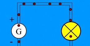
 These include all devices capable of generating, storing or converting energy. The first battery was invented and demonstrated by Alexandro Volta in 1800. It was a set of copper plates laid with damp cloth. The modified drawing began to consist of two parallel vertical lines, between which there is an ellipsis. It replaces the missing plates. If the power source consists of one element, the ellipsis is not placed.
In a constant current circuit, it is important to know where the positive voltage is. Therefore, the positive plate is made higher and the negative plate lower. Moreover, the designation of the battery on the diagram and the battery is no different.
There is also no difference in the letter code Gb. Solar batteries, which generate current under the influence of sunlight, have additional arrows in their UGO directed towards the battery.
If the power source is external, for example, the radio circuit is powered from the mains, then the power input is indicated by terminals. These can be arrows, circles with all sorts of additions. The rated voltage and type of current are indicated next to them. Alternating voltage is indicated by the “tilde” sign and may have the letter code Ac. For direct current, there is a “+” on the positive input, “-” on the negative input, or there may be a “common” sign. It is denoted by an inverted T.
Semiconductors, perhaps, have the most extensive range in radio electronics. More and more new devices are being added gradually. All of them can be divided into 3 groups:
- Diodes.
- Transistors.
- Microcircuits.
 Semiconductor devices use a p-n junction; circuit design in UGO tries to show the features of a particular device. So, a diode is capable of passing current in one direction. This property is shown schematically in the symbol. It is made in the form of a triangle, at the top of which there is a dash. This dash shows that current can only flow in the direction of the triangle.
If a short segment is attached to this straight line and it is turned in the opposite direction from the direction of the triangle, then this is already a zener diode. It is capable of passing a small current in the opposite direction. This designation is valid only for general purpose devices. For example, the image for a Schottky barrier diode is drawn with an s-shaped sign.
Some radio components have the properties of two simple devices connected together. This feature is also noted. When depicting a double-sided zener diode, both are drawn, with the vertices of the triangles directed towards each other. When designating a bidirectional diode, 2 parallel diodes are depicted, directed in different directions.
Other devices have the properties of two different parts, for example, a varicap. This is a semiconductor, so it is drawn as a triangle. However, the capacitance of its pn junction is mainly used, and these are the properties of a capacitor. Therefore, the sign of a capacitor is added to the top of the triangle - two parallel straight lines.
Signs of external factors affecting the device are also reflected. A photodiode converts sunlight into electric current, some types are elements of a solar battery. They are depicted as a diode, only in a circle, and 2 arrows are directed towards them to show the sun's rays. An LED, on the other hand, emits light, so the arrows come from the diode.
Polar and bipolar transistors
 Transistors are also semiconductor devices, but have basically two pnp junctions in bipolar transistors. The middle region between two transitions is the control region. The emitter injects charge carriers, and the collector receives them.
The body is depicted with a circle. Two p-n junctions are depicted by one segment in this circle. On the one hand, a straight line approaches this segment at an angle of 90 degrees - this is the base. On the other hand, 2 oblique straight lines. One of them has an arrow - this is the emitter, the other without an arrow is the collector.
The emitter determines the structure of the transistor. If the arrow goes towards the junction, then it is a p-n-p transistor, if it goes away from it, then it is an n-p-n transistor. Previously, a unijunction transistor was produced, it is also called a double-base diode, it has one p-n junction. It is designated as bipolar, but there is no collector and there are two bases.
The field-effect transistor has a similar pattern. The difference is that the transition is called a channel. The straight line with the arrow approaches the channel at a right angle and is called the gate. The drain and source come from the opposite side. The direction of the arrow indicates the type of channel. If the arrow is directed towards the channel, then the channel is n-type, if away from it, then it is p-type.
The insulated gate field effect transistor has some differences. The gate is drawn as a letter G and is not connected to the channel, the arrow is placed between the drain and source and has the same meaning. In transistors with two insulated gates, a second gate of the same type is added to the circuit. The drain and source are interchangeable, so the field-effect transistor can be connected in any way, you just need to connect the gate correctly.
Integrated circuits
Integrated circuits are the most complex electronic components. Conclusions are usually part of an overall scheme . They can be divided into the following types:
- analog;
- digital;
- analog-to-digital.
In the diagram they are indicated as a rectangle. Inside there is a code and (or) the name of the circuit. Outgoing terminals are numbered. Op-amps are drawn as a triangle, with the output signal coming from its apex. To count the pins, a mark is placed on the microcircuit body next to the first pin. This is usually a square-shaped recess. To correctly read microcircuits and symbol designations, tables are included.

Other items
 All radio components are connected to each other by conductors. In the diagram they are depicted as straight lines and drawn strictly horizontally and vertically. If the conductors have an electrical connection when crossing each other, then a dot is placed at this place. In Soviet and American diagrams, to show that the conductors are not connected, a semicircle is placed at the intersection.
Capacitors are indicated by two parallel lines. If it is electrolytic, for the connection of which it is important to observe polarity, then a + is placed near its positive terminal. There may be designations for electrolytic capacitors in the form of two parallel rectangles, one of them (negative) is painted black.
To designate variable capacitors, an arrow is used; it crosses out the capacitor diagonally. In trimmers, a T-shaped sign is used instead of an arrow. Varicond - a capacitor that changes capacitance depending on the applied voltage, is drawn like an alternating one, but the arrow is replaced by a short straight line, next to which there is the letter u. The capacitance is shown with a number and a microFarad (microFarad) is placed next to it. If the capacity is smaller, the letter code is omitted.
Another element that no electrical circuit can do without is a resistor. Indicated in the diagram as a rectangle. To show that the resistor is variable, an arrow is drawn on top. It can be connected either to one of the pins, or be a separate pin. For trimmers, a sign in the form of the letter t is used. As a rule, its resistance is indicated next to the resistor.

Symbols in the form of dashes can be used to indicate the power of fixed resistors. A power of 0.05 W is indicated by three oblique, 0.125 W - two oblique, 0.25 W - one oblique, 0.5 W - one longitudinal. High power is shown in Roman numerals. Due to the diversity, it is impossible to describe all the designations of electronic components on the diagram. To identify a particular radio element, use reference books.
Alphanumeric code
For simplicity, radio components are divided into groups according to characteristics. Groups are divided into types, types - into types. Below are the group codes:

For ease of installation, locations for radio components are indicated on printed circuit boards using a letter code, a picture, and numbers. For parts with polar terminals, a + is placed at the positive terminal. In places for soldering transistors, each pin is marked with a corresponding letter. Fuses and shunts are shown as straight lines. The pins of the microcircuits are marked with numbers. Each element has its own serial number, which is indicated on the board.