DS18B20. Russian description. Connecting Ds18b20 to Arduino
The DS18B20 is a digital temperature sensor. The sensor is very easy to use. First, it is digital, and secondly - it has only one contact, from which we receive a useful signal. That is, you can connect to a single Arduino at the same time a huge number of these sensors. Pins will be more than enough. Moreover, you can even connect several sensors to one pin on the Arduino! But first things first.
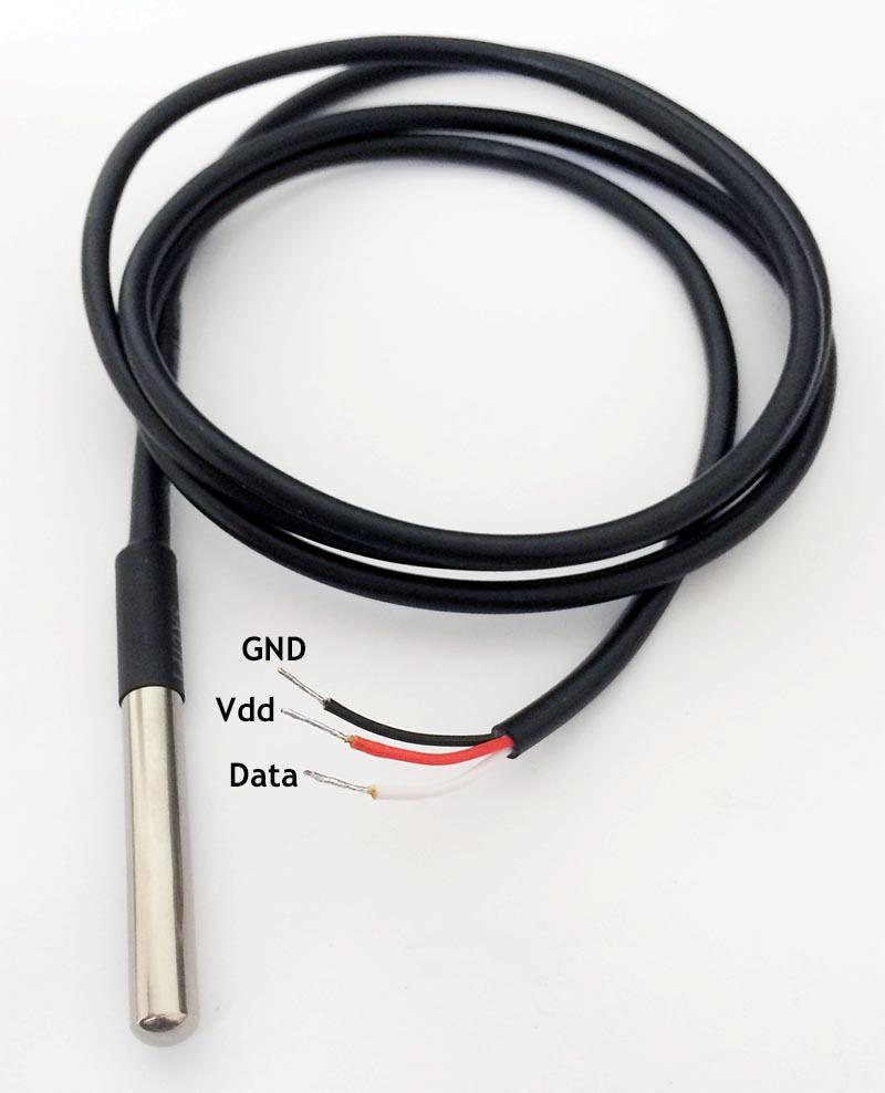
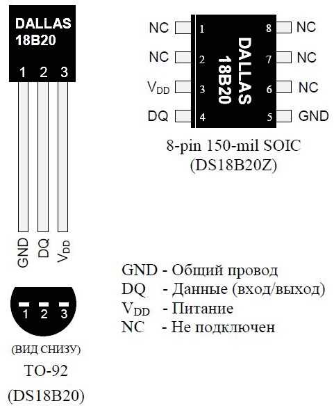
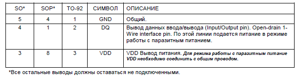
DS18B20 has various form factors. So the choice of which one to use is yours. Three options are available: 8-Pin SO (150 mils), 8-Pin µSOP, and 3-Pin TO-92. Surfing on eBay or Aliexpress shows that the Chinese are offering a TO-92 version in a waterproof case. That is, you can safely dip such a miracle in the water, use it in the rain, etc. etc. These sensors are manufactured with three output contacts (black - GND, red - Vdd and white - Data).
The various form factors of the DS18B20 sensors are shown in the figure below.
Model DS18B20 in a waterproof case:
DS18B20 is easy to use. You can power it through the contact data (in this case, you use only two of the three contacts to connect!). The sensor operates in a voltage range from 3.0 V to 5.5 V and measures temperature in the range from -55 ° C to + 125 ° C (from -67 ° F to + 257 ° F) with an accuracy of ± 0.5 ° C (from -10 ° C up to + 85 ° C).
Another cool feature: you can connect up to 127 sensors in parallel! and read the temperature readings from each separately. It is not entirely clear in which project such a thing may be needed, but you can connect two sensors and control the temperature in the refrigerator and freezer. In this case, you leave free a bunch of pins on the Arduino ... In general, the feature is nice.
What you need to control the temperature with the Arduino and DS18B20
Software
- Naturally, you need an Arduino IDE;
- Library OneWire library, which greatly facilitates the work with the Arduino and sensor DS18B20;
- Sketch...
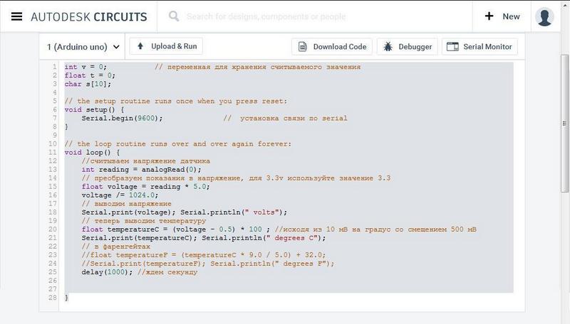
We load the sketch on Arduino
The sketch below is in the OneWire library, in the examples category. Go to “File” - “Examples” - “OneWire” and select example “DS18x20_Temperature”. The program code is presented below.
This example uses the OneWire Library to collect data from all connected DS28B20 temperature sensors (how to connect several sensors described at the end of the article) and display them in the Arduino IDE serial monitor window.
In the serial monitor window, you will see something like the following:
ROM \u003d 28 88 84 82 5 0 0 6A
No more addresses.
ROM \u003d 28 88 84 82 5 0 0 6A
Data \u003d 1 56 1 4B 46 7F FF A 10 D1 CRC \u003d D1
Temperature \u003d 21.37 Celsius, 70.47 Fahrenheit
No more addresses.
ROM \u003d 28 88 84 82 5 0 0 6A
Data \u003d 1 56 1 4B 46 7F FF A 10 D1 CRC \u003d D1
Temperature \u003d 21.37 Celsius, 70.47 Fahrenheit
Make sure you specify the correct pins!
In line 10, where “OneWire ds (2);” is indicated, a pin is set to which the data contact from the sensor is connected.
In this example, pin 2 is used, but the default pin values \u200b\u200bin the OneWire example are 10. It can also be used.
#include & ltOneWire.h & gt
// example of using the library OneWire DS18S20, DS18B20, DS1822
OneWire ds (2); // on pin 10 (4.7 kΩ resistor needed)
void setup (void) (
Serial.begin (9600);
void loop (void) (
byte present \u003d 0;
float celsius, fahrenheit;
if (! ds.search (addr)) (
Serial.println ("No more addresses.");
Serial.println ();
ds.reset_search ();
Serial.print ("ROM \u003d");
Serial.write ("");
Serial.print (addr [i], HEX);
if (OneWire :: crc8 (addr, 7)! \u003d addr) (
Serial.println ("CRC is not valid!");
Serial.println ();
// first byte identifies the chip
Serial.println ("Chip \u003d DS18S20"); // or older DS1820
Serial.println ("Chip \u003d DS18B20");
Serial.println ("Chip \u003d DS1822");
Serial.println ("Device is not a DS18x20 family device.");
ds.select (addr);
delay (1000); // 750 may be enough, but maybe not enough
// we could use ds.depower () here, but the reset will take care of it
present \u003d ds.reset ();
ds.select (addr);
Serial.print ("Data \u003d");
Serial.print (present, HEX);
Serial.print ("");
data [i] \u003d ds.read ();
Serial.print (data [i], HEX);
Serial.print ("");
Serial.print ("CRC \u003d");
Serial.print (OneWire :: crc8 (data, 8), HEX);
Serial.println ();
// convert this to actual temperature
// since the result is a 16 bit integer, it must be stored in
// variable with the data type "int16_t", which is always 16 bits,
// even if we are compiling on a 32-bit processor
int16_t raw \u003d (data
if (data \u003d\u003d 0x10) (
raw \u003d (raw & 0xFFF0) + 12 - data;
byte cfg \u003d (data & 0x60);
// for small values, small bits are not defined, let's reset them
if (cfg \u003d\u003d 0x00) raw \u003d raw & ~ 7; // resolution of 9 bits, 93.75 ms
else if (cfg \u003d\u003d 0x20) raw \u003d raw & ~ 3; // resolution of 10 bits, 187.5 ms
else if (cfg \u003d\u003d 0x40) raw \u003d raw & ~ 1; // resolution of 11 bits, 375 ms
//// default resolution is 12 bits, the conversion time is 750 ms
celsius \u003d (float) raw / 16.0;
fahrenheit \u003d celsius * 1.8 + 32.0;
Serial.print ("Temperature \u003d");
Serial.print (celsius);
Serial.print ("Celsius,");
Serial.print (fahrenheit);
Serial.println ("Fahrenheit");
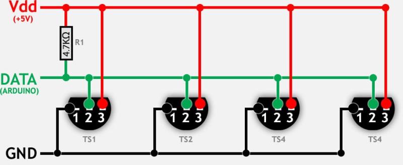
How to connect multiple DS18B20 sensors to Arduino?
You can connect multiple DS18B20 digital temperature sensors in parallel. In this case, the OneWire library will allow you to read data from all sensors simultaneously.
The following are two methods for connecting sensors.
For a large number of sensors (more than 10), it is necessary to use resistors with less resistance (for example, 1.6 KΩ or even less).
In addition, if you connect in parallel more than 10 sensors, problems may arise (errors in taking readings). Therefore, it is recommended to install an additional resistor of 100 ... 120 Ohms between the data contact on the Arduino and the data on each sensor!
The result of the previous sketch with two connected sensors can look like this:
ROM \u003d 28 88 84 82 5 0 0 6A
Data \u003d 1 51 1 4B 46 7F FF F 10 FE CRC \u003d FE
Temperature \u003d 21.06 Celsius, 69.91 Fahrenheit
ROM \u003d 28 DA CA 27 5 0 0 49
Data \u003d 1 4E 1 4B 46 7F FF 2 10 D9 CRC \u003d D9
Temperature \u003d 20.87 Celsius, 69.57 Fahrenheit
No more addresses.
Choosing the right sensor
It would be nice to know from which sensor you get the data when you use several sensors in parallel. How to do it?
Serial number
Since the sensors are digital, each of them has an individual serial number, which can be used to identify one or another sensor. It seems to be all simple. But ... we need to pre-determine these serial numbers before using them to identify the sensor, right?
You could draw on the examples above that the sketch gives us the data in the form of a 64-bit serial number - the value “ROM”. For example:
28 88 84 82 5 0 0 6A or 28 DA CA 27 5 0 0 49 in the example above.
Do not forget, if you use a large number of sensors at the same time (10 or more), you need to add 100 ... 120 Ohm resistors between the data contacts from the DS18B20 sensor and the data pin to the Arduino (for each sensor!).
Below is a diagram of parallel connection of several sensors using three contacts.
Leave your comments, questions and share your personal experience below. In the discussion often new ideas and projects are born!
In this article we will tell our readers how to connect temperature sensors. DS18B20, LM35 and TMP36on the circuit board Arduino unowhich is built on a microcontroller ATmega328. The main purpose of the temperature sensors DS18B20, LM35 and TMP36 is temperature readings. In our case, the temperature readings from these sensors will be read by the Arduino UNO printed circuit board, and output the result on a computer screen. In fact, using these sensors, anyone can create their own thermometer. In addition to a detailed description of the use of Arduino UNO and DS18B20, LM35 and TMP36 sensors, we will tell our readers where to buy these components.
We prepare the software on the PC using the Arduino IDE
If you already have an Arduino UNO board and the sensors under consideration, then it is time to configure the computer so that it can work with the microcontroller. For this task, we will need the Arduino IDE software package. Download this package on the official website www.arduino.cc. At the time of this writing, the latest version of the package is ARDUINO 1.6.10. We will use IDE on a PC with Windows 10 operating system. After downloading the IDE, we will launch the installation file.
In the initial window of the installer, we accept the terms of the license agreement and proceed to the next window.
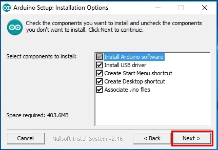
In this window, leave everything as it is and continue the installation by clicking the " Next\u003e».
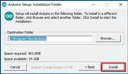
In this window, you can choose the installation path for the Arduino IDE, in our case it is the default folder. Selecting the path, press the button " Install, Which will start the installation process.
After the installation is complete, a shortcut will appear on your desktop named Arduino.
As you can see from the example, the installation of the Arduino IDE is not much different from the installation of other programs, the only thing that can confuse the user is the English interface.
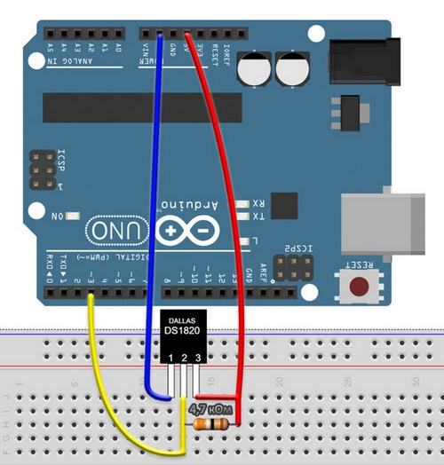
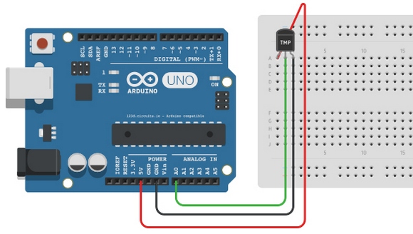
We connect the DS18B20 sensor to the Arduino UNO board
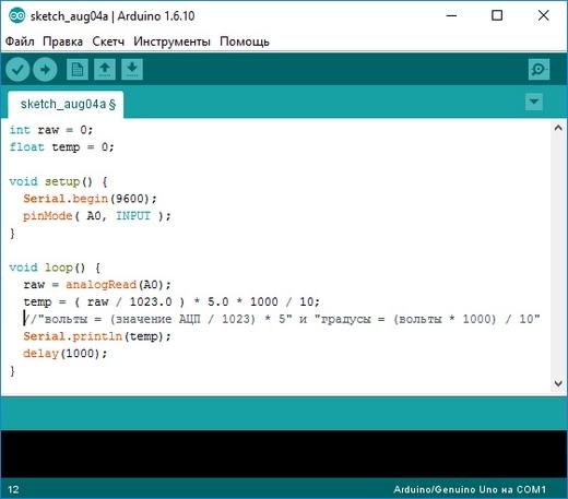
First thing we need to plugmyself sensor to board. For this we need breadboard and resistor with a resistance of 4.7 kΩ. Below is the wiring diagram of the sensor in question. DS18B20 to Arduino uno.
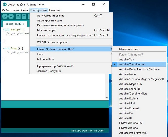
Connect the board to the computer via USB cable. After connecting, the board should light up the LED called " ON". Now we need open previously installed Arduino IDE through the shortcut on your desktop.
In the open program window, go to the menu “ Instruments"To item" Pay: ”And choose our fee.
To make our sensor work, we need load library « DallasTemperature», Which can be downloaded from this link arduino-project.net/DallasTemperature.rar. After loading the library, it needs to be connected to the IDE. To do this, unzip the downloaded library into the library directory, which is located at the address “C: \\ Program Files \\ Arduino \\ libraries”. You can view the connected library in the menu “ Sketch».
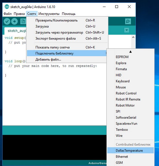
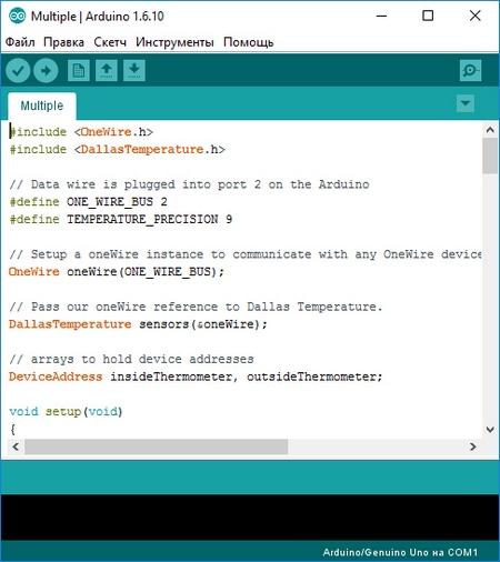
Now let's execute an example from the connected library. To do this, follow the links " File» - « Examples» - « DallasTemperature» - « Multiple". After this action, the example chosen by us will be loaded into the program window.
Now load this example into the Arduino UNO board using the "" button. Thereafter open item « Port monitor", Which is in the menu" Instruments».
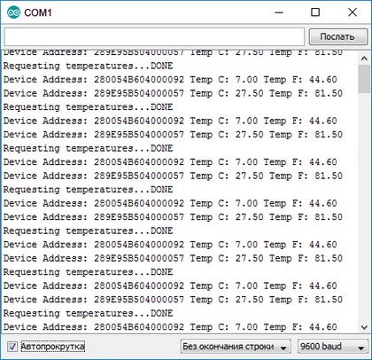
From the monitor you can see that our DS18B20 sensor shows the temperature, both in Celsius and Fahrenheit.
We connect the LM35 sensor to the Arduino UNO board
temperature sensor LM35 is an inexpensive model that the company produces Texas Instruments. This sensor is quite easy to connect to the Arduino UNO. Below is a diagram of the connection of the considered sensor to the printed circuit board.
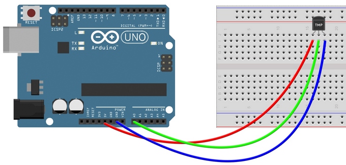
From the diagram it is clear that the sensor LM35 connects directly without using a resistor. Now we type in a fairly simple code shown in the IDE below.
After downloading this code to the board, open “ Port monitor"And see how the sensor takes temperature readings from the place where it is located.
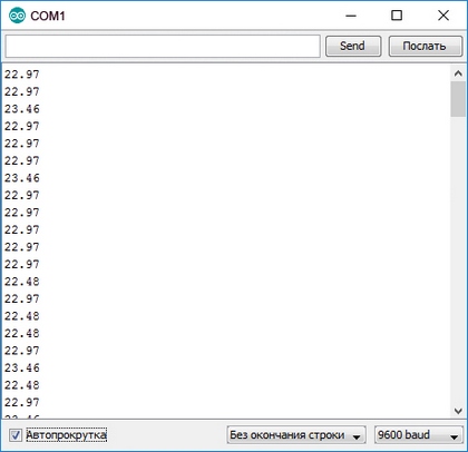
From the example it can be seen that the LM35 sensor is much easier to connect to the Arduino UNO than the one considered earlier.
We connect the TMP36 sensor to the Arduino UNO board
temperature sensor TMP36 is a budget model of the company Analog devices. Since for this example we did not have the sensor itself, we used the Internet service that allows us to emulate Arduino boards. This example will be especially interesting to those users who want to try the Arduino before purchasing it. To get to the Autodesk Circuits service, you need to go to https://circuits.io. On this page you need to go through the quick registration procedure, after which you will be taken to home page service.

To create a new project, you must press a button « New electronics lab" on this page. After this action we will get to the project window.
From the project window it is clear that we have only a breadboard. To add the components we need open the panel « Components". From this panel, we add and connect the components, as shown in the image below.
After building the package go to the panel « Code Editor"And insert textpictured below.
Also note the code. It contains descriptions of the functions of all operations. Now try to run our fee. For this press the button « Start simulation“, Then we will see how the green LED lights up. To verify that our project is working, we let's open « Serial monitor».
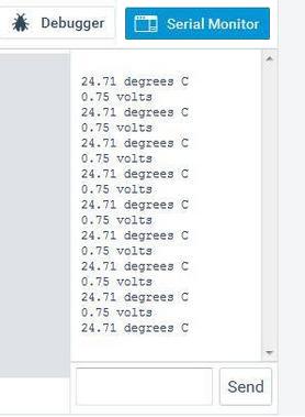
From the monitor window, you can see that our virtual sensor measures temperature readings.
From the example, it is clear that to make a project with a TMP36 sensor in Autodesk Circuits is a snap. We strongly recommend beginners to use the emulator before actually using the Arduino UNO and components.
If you incorrectly assemble any scheme, then you can actually burn both the Arduino UNO board and its components. By the way, in Autodesk Circuits you can also burn a PCB, albeit a virtual one.
Where to get the Arduino components to measure the temperature
Many more than once thought about buying Arduino and additional details to it. But the deterrent of such a purchase has always been a fairly overpriced price, which is represented in the domestic market. To save our readers, we recommend buying all Arduino components and boards in China. One of the most popular Chinese online stores is AliExpress.com. On this site you can find almost any component and fee Arduino. Below is a list of the parts that we used in the article:
- The DS18B20 temperature sensor costs $ 0.7;
- The LM35 temperature sensor costs $ 0.8;
- Temperature sensor TMP36 costs $ 3;
- An Arduino UNO PCB costs about $ 3.
From the list we can summarize that the Arduino UNO bundle plus DS18B20 is the most profitable offer.
Summarize
In this article, we looked at two examples of connecting physical sensors measuring the DS18B20, LM35 to an Arduino UNO printed circuit board. In addition, we have considered a variant of the virtual assembly of the circuit using the TMP36 sensor. In all the examples we presented the output of temperature indicators only through “ Port monitor". This was done specifically to make the assembly scheme as simple as possible. In the open spaces of the network you can find hundreds of examples where you can use these connection options:
- Transformation of a smartphone into a thermometer, thanks to the removal of temperature readings on its screen or PC from various sensors using the Wi-Fi module for Arduino;
- Transformation of a smartphone into a thermometer, due to the removal of temperature indicators on its screen or PC from various sensors using the Bluetooth module for Arduino;
- Creating a thermostat with LED display;
- Creating a thermometer based on Arduino and TFT display;
- Get temperature readings with Arduino over the Internet.
This is only a small fraction of the examples by which the user can get temperature indicators through the Arduino board. Using Arduino, in our time, everyone can translate into reality the concept of a smart home. We hope our material will be useful for you, and thanks to it, you can connect temperature sensors to your Arduino board.
Related videos
The article provides a detailed description of the integrated temperature sensor DS18B20 in Russian. The information has been translated into Russian from the official documentation of the sensor manufacturer - Dallas Semiconductor.
General description.
The DS18B20 is a digital temperature meter with a resolution of 9 to 12 bits and a temperature control alarm function. Control parameters can be set by the user and saved in the non-volatile memory of the sensor.
DS18B20 communicates with the microcontroller via a single-wire communication line using the 1-Wire interface protocol.
The temperature measurement range is from -55 to +125 ° C. For the range from -10 to +85 ° C, the error does not exceed 0.5 ° C.
Each DS18B20 chip has a unique 64-bit serial code that allows multiple sensors to connect to one common communication line. Those. through one port of the microcontroller, you can exchange data with several sensors distributed at a considerable distance. The mode is extremely convenient for use in environmental control systems, temperature monitoring in buildings, equipment nodes.
Briefly about the features of DS18B20.
- For a single-wire 1-Wire interface, one communication port with the controller is sufficient.
- Each device has a unique serial code of 64 bits in length.
- The ability to connect multiple sensors through a single communication line.
- No need for external components.
- The ability to receive power directly from the communication line. Power supply within 3.0 V ... 5.5 V.
- Temperature measurement range is -55 ... +125 ° C.
- The error does not exceed 0.5 ° C in the range of -10 ... +85 ° C.
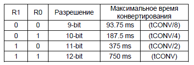
- Conversion resolution 9… 12 bits. Set by user.
- The measurement time does not exceed 750 ms, with the maximum possible resolution of 12 bits.
- The possibility of programming alarm parameters.
- The alarm signal transmits the address of the sensor, whose temperature is outside the specified limits.
- Software compatibility with DS1822.
- Extremely wide applications.
Purpose of conclusions.
DS18B20 Sensor Overview
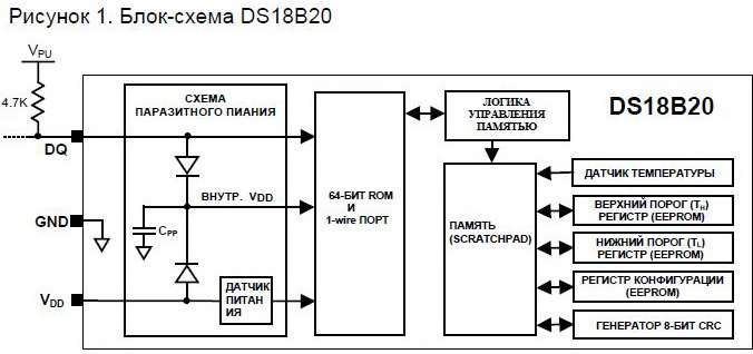
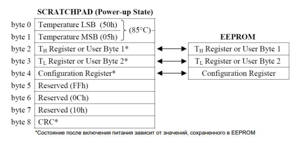
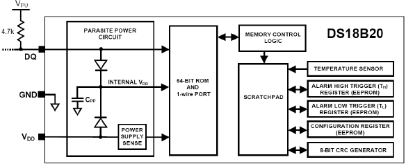
Figure 1 is a block diagram of a DS18B20 sensor. 64-bit ROM (ROM) stores the unique serial code of the device. RAM contains:
- measured temperature value (2 bytes);
- upper and lower alarm thresholds (Th, Tl);
- configuration register (1 byte).
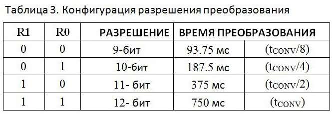
Through the configuration register, you can set the resolution of the temperature sensor conversion. Resolution can be set to 9, 10, 11 or 12 bits. The configuration register and alarm thresholds are contained in non-volatile memory (EEPROM).
Mode - temperature measurement.
The main function of the DS18B20 is to convert the sensor temperature to a digital code. The resolution of the conversion is set to 9, 10, 11 or 12 bits. This corresponds to a resolution of 0.5 (1/2) ° C, 0.25 (1/4) ° C, 0.125 (1/8) ° C, and 0.0625 (1/16) ° C. At power up, the state of the configuration register is set to a resolution of 12 bits.
After power on, the DS18B20 is in a low-power resting state. To initiate a temperature measurement, the master (microcontroller) must execute the TEMPERATURE TRANSFORMATION command. After the conversion is completed, the temperature measurement result will be in 2 bytes of the temperature register, and the sensor will again go into a state of rest.
If the DS18B20 is turned on with an external power supply, the wizard can monitor the status of the conversion command. To do this, it must read the state of the line (perform the time slot reading), upon completion of the command, the line goes into a high state. During the execution of a conversion command, the line is kept in a low state.
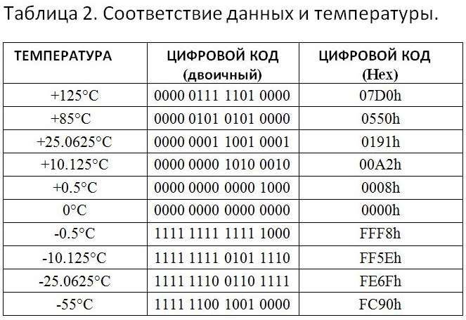
The DS18B20 measures temperature in degrees Celsius. The measurement result is represented as a 16-bit signed value in the additional code (Fig. 2.). The sign bit (S) is 0 for positive numbers and 1 for negative numbers. With a resolution of 12 bits, the temperature register has all the bits significant, i.e. have reliable values. For resolution of 11 bits, bit 0 is not defined. For 10-bit resolution bits 0, 1 are not defined. At resolution of 9 bits, bits 0, 1, and 2 have a reliable value. Table 2 shows examples of the correspondence between digital codes and temperature values.
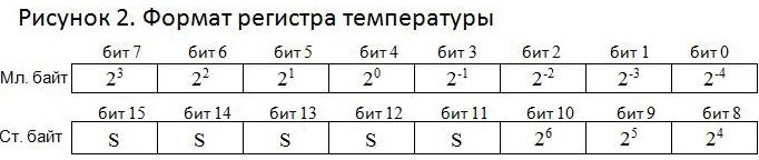
For people not experienced in binary mathematics, I will write that to calculate the temperature you need:
- If the value is positive (S \u003d 0), the code should be converted to decimal and multiplied by 0.0625 ° C.
- If the value is negative (S \u003d 1), the additional code must first be converted into a straight line. To do this, invert each digit of the binary code and add 1. And then convert to decimal and multiply by 0.0625 ° C.
The mode is alarm transmission.
After executing the temperature conversion command, the measured value is compared with the upper and lower thresholds from the Th, Tl registers (format in Figure 3). These are byte values, signed, in the additional code, S \u003d 0 means that the number is positive, and S \u003d 1 is negative. Threshold values \u200b\u200bare stored in non-volatile memory (EEPROM). Th and Tl are available for reading and writing through bytes 2, 3 of RAM. Details about this in the section.
Due to the different lengths of the TH, TL and temperature registers, they are compared only with bits 11 through 4 of the temperature register. If the value of the measured temperature exceeds TH or is lower than TL, then a symptom of an accident in DS18B20 is formed. The sign is overwritten with every temperature measurement, and if the temperature returns to the specified limits, it is reset.
The master can check the status of the alarm sign with the ALARM SEARCH command. Any sensor with an active tag will respond to a search command. Thus, the wizard will determine exactly which DS18B20 generates an alarm. After changing the values \u200b\u200bof the TH and TL registers, only the next temperature conversion will generate a reliable sign of alarm.
Power supply DS18B20.
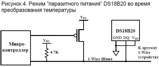
However, when the DS18B20 performs a temperature transform or copy data memory to an EEPROM, the current consumption can reach 1.5 mA. Such a current can cause a decrease in the supply voltage of the device to an inadmissible value. The current of the pull-up resistor and the energy stored at Cpp is not enough to power in these two modes. In order to guarantee sufficient power to the device, it is necessary to provide a powerful bus pull up to a high level at the time when temperature conversion or copying of the memory data to the EEPROM occurs. This can be done using a MOSFET transistor, as shown in the diagram (Figure 4). The data bus must be connected to a powerful power supply:
- within 10 µs after the commands CONVERTING and COPYING MEMORY;
- during the conversion time (tconv) and data transfer (at least t WR \u003d 10 ms).
No other operations at this time on the bus can not be allowed.
As a rule, modern microcontrollers have a high output current level enough to power the DS18B20. Then there is no need for a MOSFET transistor.
A common method can be used to power the DS18B20 - connecting external power through the V DD pin (Figure 5). The obvious advantages of this method are that there is no need for a MOSFET transistor and that during the conversion the bus remains free and can be used for other purposes.
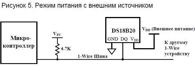
I, in such cases, use the following connection scheme DS18B20.
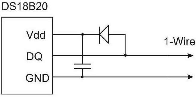
In this scheme, the thermal sensor operates in an external power supply mode, which is stored on an additional capacitor through a diode. In my devices, the circuit works fine.
64-bit device serial code.
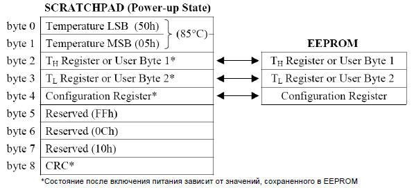
Sensor memory.
The organization of the DS18B20 memory is shown in Figure 7. All memory includes operational (SRAM) and non-volatile (EEPROM) memory. The EEPROM stores the TH, TL registers and the configuration register. If the alarm function is not used, then the TH and TL registers can be used as general registers. All memory management commands are described in detail in the section.
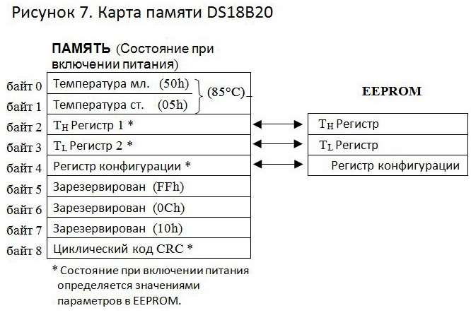
In bytes with addresses 0 and 1, the low and high bytes of the measured temperature register are stored. These bytes are read only. 2nd and 3rd bytes - TH and TL registers. Byte 4 is the configuration register. Details about this register in the section REGISTRATION OF CONFIGURATION. Bytes 5, 6, 7 are reserved, cannot be written and, when reading, always return 1.
Byte 8 is read only. It contains a cyclic code (CRC) for the first eight bytes. DS18B20 generates this code according to the method described in the section.
Data writing in bytes 2, 3 and 4 is done with the RECORD MEMORY command. Data must be transmitted starting from the low bit of byte 2. To check the data record, you can read the memory with the command READ MEMORY [BEh code]. When reading, data is transmitted over the bus, in sequence starting with the low bit of byte 0. The TH, TL data and the configuration register are written to the EEPROM at the command COPYING THE MEMORY.
When power is turned on, data from non-volatile EEPROM memory is reloaded into RAM (SRAM). Data reloading from EEPROM can also be done with the RESET command E 2. The wizard must monitor the bus status to determine when the reboot is complete. A low reading slot means that the reboot is not over yet. Upon completion of the reboot, the DS18B20 transmits reading slot 1.
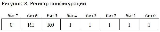
The configuration register of the thermal sensor.
Memory byte 4 is the configuration register (format in Figure 8). Bit R0, R1, you can set the resolution of the conversion (codes in Table 3). At power on, the state of the bits R0, R1 \u003d 11, which corresponds to a resolution of 12 bits. It must be remembered that there is a direct dependence of the conversion time on the resolution. Bits 7 and 0 ... 4 are reserved, cannot be used, return 1 when reading.
Cyclic code generation (CRC)
The cyclic code byte (CRC) is located in the 64-bit ROM code and in the ninth byte of SRAM memory. The ROM loop code is calculated for 56 bits of ROM code and is located in the high byte ROM. The cyclic code from SRAM is calculated from bytes 0 ... 7 SRAM. Cyclic code allows you to monitor the correctness of reading data from the DS18B20. The wizard calculates the cyclic code for the received data and compares it with the received code. Based on this, a decision is made on the correctness of the data.
The generator polynomial of a cyclic code looks like this:
C R C \u003d X 8 + X 5 + X 4 + 1
The master can calculate the cyclic code using a generator of a polynomial, according to the diagram in Figure 9. It consists of a shift register and exclusive-OR logic elements. The shift register is initially in the 0 state. The bits go into the shift register, starting with the low-order bit, the code from the ROM or from the SRAM, one bit per shift cycle. After shifting the 56th bit of the ROM or the high bit of the 7th byte of SRAM, the shift register will contain the calculated cyclic code. If the 8 bits of the ROM or SRAM received from the DS18B20 are shifted to the generator, then in case of correct data, the shift register will contain all 0.
1-Wire single-wire interface
A 1-Wire bus system consists of one master device (MASTER), which controls one or more slave devices (SLAIV). DS18B20 can only be slave. A system in which one slave is called a single point device. Multi-slave system - multipoint. All commands and exchange data are transmitted via the low-order bit forward. In the further information about the 1-Wire interface, there are three sections: hardware configuration, sequence of operations, and signals (types and time requirements).
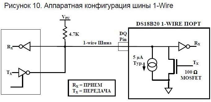
Hardware configuration
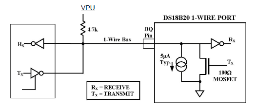
The 1-Wire interface has one link. Each device (master or slave) is connected to the data bus by a port with an open collector or tri-state output. This configuration allows each device of the system not to occupy the communication line when it is not active, and to keep the bus free for other devices. In the chip DS18B20 output (DQ) - open drain. Its equivalent circuit is shown in Fig. 10. The 1-Wire bus requires the use of an external pull-up resistor with a resistance of approximately 5 kΩ to ensure a high signal level when the devices are inactive. If the operation is to be suspended, the tire must be set to the inactive state until the next operation. A tire can be in a high state for an arbitrarily long time. Putting the bus into a low state for more than 480 µs will cause all system components to be reset.
Sequence of operations.
The sequence of operations for accessing the DS18B20 thermal sensor looks like this.
- Initialization.
- ROM command (required for any data exchange).
- Functional team (required for any data exchange).
Such a sequence must be strictly observed. Otherwise, the DS18B20 will not respond to commands. The exceptions are the ROM SEARCH command [F0h code] and TROUBLE SEARCH [ECh code]. After the formation of these two commands, the master device (master) should return to the first step (initialization).
Initialization.
Bus exchange always begins with an INITIALIZATION operation. For initialization, the master device generates a reset pulse, followed by a presence pulse from the slave device. The presence pulse informs the master that the slave is present in the system and is ready to perform the operation. The timing of the reset and presence pulses are described in section.
Commands ROM codes.
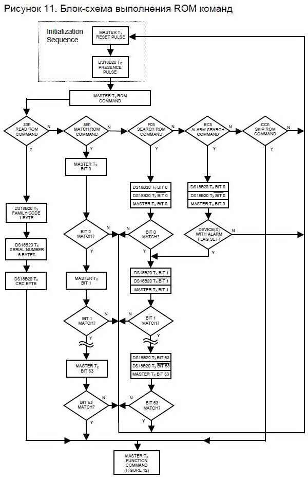
After the master device receives a presence impulse, it can operate with ROM commands. These are commands for operations with 64-bit individual codes of each slave device. They allow the master to select a particular slave among many others. Also, using these commands, you can find out how many slave devices are connected to the bus, their types, select devices in alarm state. There are 5 ROM commands, 8 bits each. The master must send the ROM command before executing the DS18B20 functional commands. A block diagram of the execution of ROM commands is depicted in Figure 11.
ROM search
After power-up, the master device must read the ROM codes of all slave devices connected to the bus. This will determine the number of slaves and their types. The master device learns ROM codes through the process of identifying the codes of each device on the bus. It must execute the ROM search command as many times as necessary to identify all slave devices. With one slave in the system, it is easier to use the ROM READ command. After the ROM search, the bus operation should begin again with initialization.
ROM read
The command is used in single point systems with one slave device. It allows the master device to read the 64-bit ROM code, without using the ROM SEARCH command. Using the Read ROM command in a multipoint system will result in data conflicts between slaves.
ROM match
The command COMBINE ROM, after which the 64-bit ROM code must follow, allows the master to access a specific slave device. Only one slave device whose code matches the transmitted code will react to the functional commands. Other slave devices will be inactive until the next reset pulse.
ROM Skip
The command allows the master device to access all devices on the bus at the same time, without using ROM codes. For example, you can run a temperature conversion operation on all devices by executing the ROM PASS command, and then TEMPERATURE CONVERSION. The READ MEMORY command can follow the ROM PASS command only with one slave device connected to the communication line. Such a sequence of commands significantly saves the time of the exchange with the sensors. It is especially effective when used in the system of a single slave device.
Alarm search
The command acts identically to the SEARCH ROM command. It differs in that only slaves in an alarm state will respond to it. The command allows the slave device to determine which thermal sensors are in an alarm state after the last temperature conversion. After each ALARM SEARCH, you must return to INITIALIZATION.
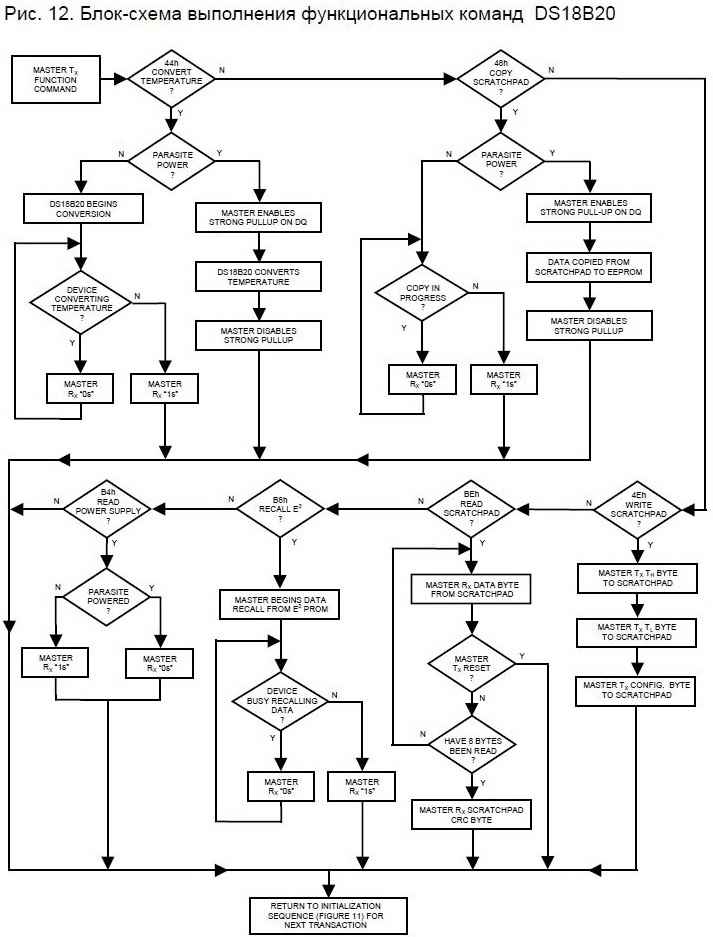
Functional Team Group
After executing the ROM command to select the DS18B20 with the desired code, the master device can send functional commands to the sensor. They allow you to write and read data from the DS18B20 RAM, initiate temperature conversion and determine the power mode. The functional commands of DS18B20 are described below, summarized in Table 4, the algorithm for working with them is shown in Figure 12.
Temperature conversion
Memory record
The command allows you to load 3 bytes into the operational memory of the sensor. The first byte is written to the Th register (2 bytes of memory), the second byte to Th (byte 3 of memory) and the third byte to the configuration register (byte 4). The master transmits data starting with the low-order bit. All three bytes must be written before the master generates a reset signal.
Reading memory
The command is used to read device memory. Data transfer occurs from the low bit of memory byte 0, and continues until all 9 bytes are read. If only part of the data is required, the master can interrupt the transmission, creating a reset pulse.
Copy memory
The command reloads the values \u200b\u200bof the Th, Tl registers and the configuration register from the EEPROM into RAM. After sending the RESET command, the master can execute the read slot, and the DS18B20 will report the reload status. A transfer of 0 will mean that the operation is still in progress, 1 means that the operation is completed. The reboot operation automatically occurs upon power up. Therefore, the RAM contains reliable data immediately after the power supply.
Reading Diet
Table 4. Functional commands DS18B20.
| TEAM | DESCRIPTION | CODE | OPERATIONS ON THE BUS | NOTES |
| TEAM CONVERTING TEMPERATURE | ||||
| Temperature measurement | Initializes temperature measurement | 44h | DS18B20 transmits the temperature conversion operation to the master | 1 |
| TEAMS OF WORK WITH MEMORY | ||||
| Reading memory | Reads all RAM, including CRC loop code | Beh | DS18B20 sends to the master up to 9 bytes | 2 |
| Memory record | Writes bytes 2, 3 and 4 to RAM (TH, TL and configuration register) |
4Eh | The master transmits 3 bytes to the DS18B20. | 3 |
| Copy memory | Copies TH, TL, and configuration register from RAM to EEPROM | 48h | 1 | |
| Overloads TH, TL, and configuration register from EEPROM to main memory. | B8h | DS18B20 passes the reboot status to the master. | ||
| Reading Diet | Informs the master about the power mode of the DS18B20. | B4h | DS18B20 hands on power to master | |
Notes.
Interface 1-Wire
The DS18B20 uses the 1-Wire interface protocol for data exchange, which provides data integrity control. This protocol defines the signals:
- reset pulse
- presence impulse
- write bit with value 0,
- write bit with value 1,
- read bit with a value of 0,
- read bits with a value of 1.
All these signals, except for the presence pulse, form the master device.
Initialization - reset and presence pulses
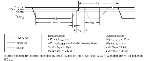
Any DS18B20 communication operations begin with an initialization sequence, which consists of a reset pulse from the master device to the slave, and a response presence pulse from the DS18B20. This process is shown in Figure 13. The thermal sensor sends a presence pulse in response to a reset pulse to inform the master that it is connected to the bus and is ready for use.
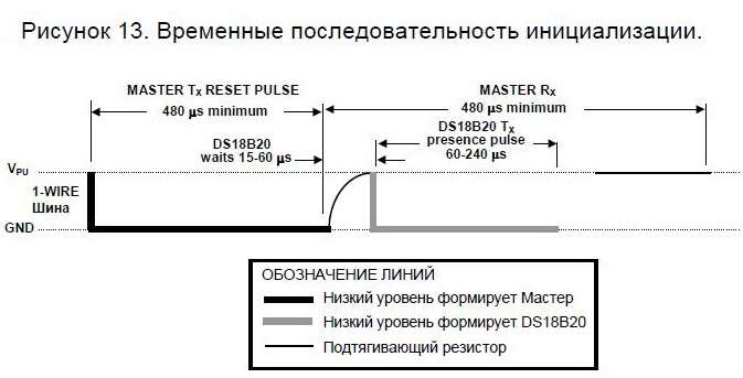
During the initialization sequence, the master transmits a reset pulse (Tx), generating a low level signal on the bus for at least 480 µs. Next, the master device releases the bus and goes into receive mode (Rx). When the bus is released, it pulls up to a high logic level with a 5 kΩ resistor. The sensor emits a positive front, waits 15-60 μs and transmits a pulse of presence, keeping the line low for 60-240 μs.
Time slots for reading and writing.
Data exchange on the 1-Wire bus occurs in time slots (time slots). One time slot transmits one bit of information.
Time slots recording.
The protocol defines two types of time slots for recording data in the DS18B20: for recording the value 1 and recording the value 0. The recording slot is not less than 60 μs with a pause for recovery between slots 1.0 μs, at least. Any recording slot is initiated by a negative edge of the bus signal (Fig. 14).
To form a recording slot 1, after transferring the bus to a low state, the master must release the bus for 15 µs. A 5 kΩ pull-up resistor will create a high voltage on the bus.
In order to form a recording slot 0, after the bus is brought to a low state, the master device must continue to keep the bus in a low state throughout the entire slot time (at least 60 μs).
The DS18B20 checks the state of the signal in a time interval between 15 and 60 μs, counting it from the beginning of the recording slot. The bus condition on this segment corresponds to the value of the bit to write to the sensor.
Time slots reading.
The length of the read slot, as well as the write slot, must be at least 60 μs with a pause for recovery between slots 1 μs, at a minimum. Any read slot is initiated by a negative edge of the bus signal (Figure 14).
After the master has initialized the read slot, the DS18B20 transmits a data bit. For transmission, 1 sensor leaves the bus free (in high condition), and for transmission 0, it forms a low level on the bus.
When transmitting 0, the DS18B20 should free the bus at the end of the slot. A pull-up resistor will form a high level on it. The output of the DS18B20 is reliable for 15 µs, from the start of the read slot.
In fig. 15 shows that the total amount of time slots for the Tinit, TRC and TSAMPLE read slot should be no more than 15 µs.
Fig. 16 shows that for maximum reliability of data reception, it is necessary to reduce Tinit and TRC and read the state of the bus at the end of the 15 µs segment.
Example 1 working with DS18B20.
MASTER MODE
EXPLANATION
Example 2 of working with DS18B20.
|
MASTER MODE |
TIRE DATA |
EXPLANATION |
| Tx | Reset | The master generates a reset pulse. |
| Rx | Presence | |
| Tx | CCh | |
| Tx | 4Eh | The wizard executes the write memory command. |
| Tx | 9 bytes of data | The master sends three bytes (TH, TL, and the configuration register). |
| Tx | Reset | The master generates a reset pulse. |
| Rx | Presence | DS18B20 responds with a presence pulse. |
| Tx | CCh | The wizard executes the skip ROM command. |
| Tx | Beh | The wizard sends a read memory command. |
| Rx | 9 bytes of data | The master reads all RAM, including the CRC loop code. It then calculates the CRC for the first eight bytes and compares it with the received code. If the codes are not equal, the master repeats the read operation. |
| Tx | Reset | The master generates a reset pulse. |
| Rx | Presence | DS18B20 responds with a presence pulse. |
| Tx | CCh | The wizard executes the skip ROM command. |
| Tx | 48h | The master executes the copy memory command. |
| Tx | DQ line is connected to the power bus | The wizard connects the DQ to the power bus for the duration of the conversion. |
Maximum allowable parameters DS18B20
The limiting values \u200b\u200bof the parameters are indicated. Excess of these parameters is unacceptable. Operating for a long time with the limiting values \u200b\u200bof the parameters may reduce the reliability of the device.
Notes:
Electrical characteristics of the EEPROM of alternating current (- 55 ... + 125 ° C, V DD \u003d 3.0 ... 5.5 V).
| PARAMETER | SYMBOL | CONDITIONS | MIN. | TYPE OF. | MAX. | UNIT Mod. |
| Write cycle time | t wr | 2 | 10 | ms | ||
| Number of records | N EEWR | -55 ° C - + 55 ° C | 50000 | cycle | ||
| Storage time | t EEDR | -55 ° C - + 55 ° C | 10 | years old |
Electrical characteristics of alternating current (- 55 ... + 125 ° C, V DD \u003d 3.0 ... 5.5 V).
| PARAMETER | SYMBOL | CONDITIONS | MIN. | TYPE OF. | MAX. | UNIT Mod. | NOTE Chany |
| Temperature conversion time | t CONV | 9 bit resolution | 93.75 | ms | 1 | ||
| resolution 10 bits |
187.5 | ms | 1 | ||||
| resolution 11 bits |
375 | ms | 1 | ||||
| resolution 12 bits |
750 | ms | 1 | ||||
| Power connection time | t spon | Sending a temperature conversion command | 10 | ms | |||
| Slot time | t SLOT | 60 | 120 | ms | 1 | ||
| Recovery time | t REC | 1 | ms | 1 | |||
| Recording time 0 | r LOW0 | 60 | 120 | ms | 1 | ||
| Recording time 1 | t LOW1 | 1 | 15 | ms | 1 | ||
| Data reading time | t RDV | 15 | ms | 1 | |||
| High reset time | t rsth | 480 | ms | 1 | |||
| Low reset time | t rstl | 480 | ms | 1,2 | |||
| High attendance time | t PDHIGH | 15 | 60 | ms | 1 | ||
| Low attendance time | t PDLOW | 60 | 240 | ms | 1 | ||
| Capacity | C IN / OUT | 25 | pcf |
Notes:
Figure 18. Time diagrams.
The description turned out great. With sensors to work is not easy. They require fairly complex software functions, but from a hardware point of view, the DS18B20 simply connects, measures accurately, does not require an ADC, etc.
As an example of using DS18B20 thermal sensors, I can cite my development. Two thermal sensors are used. One measures the air temperature in, the second - the temperature of the radiator.
DS18B20 digital temperature sensor that works using the 1-Wire protocol. Used when developing a home weather station on the Arduino.
DS18B20 Sensor Description
DS18B20 is a digital thermometer with a programmable resolution of 9 to 12 bits, which can be stored in the device's EEPROM. DS18B20 communicates over the 1-Wire bus and can be both the only device on the line and work in a group. All processes on the bus are controlled by a central microprocessor.
The sensor's measuring range is from –55 to +125 ° C and an accuracy of 0.5 ° C in the range from –10 to +85 ° C. In addition, the DS18B20 can be powered by a data line voltage in the absence of an external voltage source.
Each DS18B20 sensor has a unique 64-bit serial code that allows you to communicate with multiple DS18B20 sensors installed on the same bus. The first 8 bits are the serial code (for DS18B20 - 28h), then 48 bits of the unique number, and at the end 8 bits of the CRC code. This principle allows the use of a single microprocessor to monitor a variety of DS18B20 sensors distributed over a large area.
DS18S20 sensor features:
- 1-Wire interface;
- measured temperature from –55 to +125 ° C;
- accuracy of 0.5 ° C in the range from –10 to +85 ° C;
- temperature reads 9 data bits;
- time for temperature conversion - 750 ms (maximum).
The temperature data is stored in the RAM of the sensor. The memory consists of an operative ROM and a non-volatile EEPROM:
The first two bytes - contain data on the measured temperature;
The third and fourth bytes store the upper (TH) and lower (TL) temperature limits;
The fifth and sixth are not used;
Seventh and eighth - bytes counters. They can be used to more accurately measure temperature;
The ninth byte stores the CRC code of the previous eight.
 |
In addition to general commands for all types of 1-Wire devices presented in the table, the sensor can execute the following commands:
Alarm Search - the operation of this command is identical to the operation of address search, except that in this case only those sensors will respond that had the temperature exceeded the set limits during the last measurement (above TH or below TL);
Convert t - convert temperature. The sensor will measure and record current temperature data. If the master device sends read time slots for this command, while the conversion is not completed, the DS18S20 will issue a “0” to the line, and after the conversion is completed, “1”.
Write Scratchpad - write to memory. This command allows you to write 3 bytes in the sensor memory. The first byte is written to TH, the second to TL, and the third byte is written to the fifth byte of memory — this is the configuration byte;
Read Scratchpad - reading memory. The command allows us to read the sensor memory. In response to this command, the sensor will return 9 bytes of its memory, starting with the 0th byte of TEMPERATURE LSB and ending with the eighth - CRC;
Copy scratchpad - copy memory. The sensor will copy the contents of the RAM - TH and TL into the EEPROM.
The sequence of commands to obtain data from the sensor about the temperature:
Perform RESET and search for devices on the 1-Wire line.
Issue command 0x44 to start temperature conversion by the sensor.
Wait at least 750 ms.
You can use the OneWire library to work with sensors with the 1-Wire interface.
The sample for receiving data from the DS18B20 temperature sensor and data output to the serial port using the OneWire library is presented in the example
Sketch code
#include
OneWire ds (10); // 1-Wire line will be on pin 10
void setup (void)
Serial.begin (9600);
byte present \u003d 0; byte data; byte addr;
if (! ds.search (addr)) (Serial.print ("No more addresses. \\ n"); ds.reset_search ();
if (OneWire :: crc8 (addr, 7)! \u003d addr) (Serial.print ("CRC is not valid! \\ n"); return;
if (addr! \u003d 0x28) (
Serial.print ("Device is not a DS18B20 family device. \\ N"); return;
ds.reset (); ds.select (addr);
ds.write (0x44,1); // start the conversion delay (750); // waiting for 750ms
present \u003d ds.reset (); ds.select (addr);
ds.write (0xBE); // read sensor RAM
for (i \u003d 0; i< 9; i++) { // обрабатываем 9 байт data[i] = ds.read();
Serial.print (data [i], HEX); Serial.print ("");
// calculate the temperature :)
int HighByte, LowByte, TReading, Tc_100; LowByte \u003d data;
Serial.print ("LB \u003d"); Serial.print (LowByte, HEX); HighByte \u003d data;
Serial.print ("HB \u003d"); Serial.print (HighByte, HEX); TReading \u003d (HighByte<< 8) + LowByte;
Tc_100 \u003d TReading / 2;
Serial.print ("T \u003d"); Serial.print (Tc_100); Serial.println ();
Details Created 10/09/2015 7:34 PM
APPEARANCE AND PURPOSE OF CONCLUSIONS
STRUCTURAL SCHEME
DS18B20 has:
- read-only memory with 64-bit unique instrument code;
- a memory containing a 2-byte temperature register that stores the temperature value at the end of the temperature conversion, two single-byte temperature control registers TH and TL, and a configuration register.
The configuration register allows the user to set the resolution of the temperature digitizer to 9, 10, 11, or 12 bits. With an increase in the resolution of the sensor, the time of temperature conversion also increases. The TH, TL registers and the configuration register are non-volatile (EEPROM), so they will save data when the device is turned off.
The DS18B20 uses a 1-Wire bus that uses a single data line. The bus must be connected to the power supply via a pull-up resistor. Using this bus, the microcontroller identifies and accesses temperature sensors using a 64-bit instrument code. Since each device has a unique code, the number of devices that can be accessed on one bus is virtually unlimited.
MODE - TEMPERATURE CONVERSION
The resolution of the temperature transducer can be changed by the user and is 9, 10, 11, or 12 bits, which allows temperature conversion with a resolution of 0.5 ° C, 0.25 ° C, 0.125 ° C, and 0.0625 ° C, respectively. The default resolution is set to 12-bit.
The output temperature data DS18B20 is calibrated in degrees Celsius. Temperature data is stored as a 16-bit signed number. The S bits indicate whether the temperature is positive or negative: for positive values, S \u003d 0, and for negative values, S \u003d 1. If DS18B20 is configured to convert with 12-bit resolution, then all bits in the temperature register will contain valid data . For 11-bit resolution, bit 0 is undefined. For 10-bit resolution, bits 1 and 0 are undefined, and for 9-bit resolution, bits 2, 1, and 0 are undefined.
Table 2 gives examples of digital output data and the corresponding temperature, for 12-bit resolution.
FORMAT TEMPERATURE REGISTER
Examples of the correspondence of the digital conversion data and the corresponding temperature at 12-bit resolution.
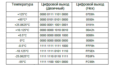
* when power is supplied to the temperature register, the number +85 о С is recorded
After DS18B20 performs a temperature conversion, the temperature value is compared with the value written to the TH and TL registers. For comparison, only bits 4-11 from the temperature register (integer temperature value) are used. If the measured temperature is lower than or equal to TL or higher than or equal to TH, an Alarm condition is formed and the Alarm flag is set in DS18B20. This flag is updated after each temperature conversion; therefore, if the Failure condition disappears, the flag will be cleared after the next temperature conversion.
Format of registers TH and TL
The master device can check the condition of the Failure of all DS18B20 on the bus by issuing the Search Failure command. Any DS18B20 with the Alarm flag set will respond to this command, so the host can determine exactly which DS18B20 are in the Alarm state. If the value of the TH or TL registers is changed, then a new temperature conversion must be started in order to check the temperature control conditions specified in the TH or TL registers.
DS18B20 Power Supply
When the DS18B20 performs temperature conversions or copies data from RAM to the EEPROM memory, it can consume up to 1.5 mA. This current can cause an unacceptable reduction in the voltage on the bus fed through a resistor. In order to ensure that the DS18B20 has sufficient supply current, it is necessary to provide high-precision power to the bus every time there is a temperature conversion or a data write operation to the EEPROM is performed. This can be achieved by using a MOSFET transistor to power the bus directly from Vpu, as shown in the figure.
The 1-Wire bus should be switched to high-precision power within 10 µs (maximum) after the Convert T temperature conversion command or the Copy Scratchpad command (copy data to EEPROM). The bus must be switched to high-precision power at the time of conversion (tconv) or data transfer (twr \u003d 10ms). No bus operations should be performed when the high-precision power mode is on.
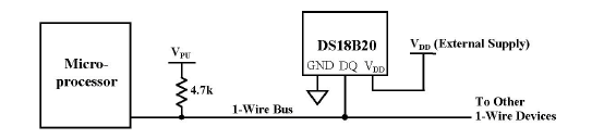
The DS18B20 can be powered in the usual way, i.e. connecting the external power wire to the VDD terminal. as shown in the figure above. The advantage of this method is that there is no need to use a MOSFET transistor. And on the bus data can be transmitted during the time of temperature conversion.
64-BIT sensor code
Each DS18B20 contains a unique 64-bit code stored in ROM. The lower 8 bits of the code contain the 1-Wire family code. The DS18B20 family code is 28h. The next 48 bits contain a unique serial number. The upper 8 bits contain cyclic redundancy check (CRC) bytes, which is calculated from the first 56 bits of the ROM code. The 64-bit ROM code and the associated ROM function control the logic that allows the DS18B20 to operate as a 1-Wire device using the protocol detailed in section 1-WIRE BUS SYSTEM.
MEMORY
Memory DS18B20 is organized as shown in the figure below. The memory consists of an operational SRAM memory and non-volatile EEPROM memory. The first two registers are the temperature conversion result registers, followed by the upper and lower temperature alarm registers (TH and TL) and the configuration register. Note that if the DS18B20 Alarm function is not used, then the TH and TL registers can be cells of universal memory.
Byte 0 and byte 1 of RAM contains the low and high bits of the temperature register, respectively. These bytes are read only. Bytes 2 and 3 provide access to the TH and TL registers. Byte 4 contains the configuration register data, bytes 5, 6, and 7 are reserved for internal use by the device and writing to these registers is impossible; when reading, these bytes will return “1” in all digits. Bytes 8 are read-only RAM and contain the cyclic redundancy check (CRC) code calculated for bytes 0-7 of RAM. The DS18B20 generates cyclic redundancy monitoring using the method described in the generation of cyclic redundancy check.
To write data into bytes 2, 3, and 4 of RAM, use the Write Scratchpad command; data must be transmitted to DS18B20, starting with byte 2. To verify the correctness of the data record, you must perform a read (using the Read Scratchpad read command) after the data has been written. Note that when reading data, the DS18B20 starts transmitting at 0 bytes. In order to save the TH, TL and configuration register data in the EEPROM, the control device must issue the Copy Scratchpad command. The data stored in the EEPROM registers is reset in RAM upon power up.
Data can be reloaded from EEPROM to RAM at any time using the Recall E2 command. The control unit can control the Recall E2 operation (the process of calling data from the EEPROM to RAM) by issuing a clock pulse after the command and monitoring the bus status, if 0 — the reboot operation continues, if 1 — the process is completed.
DS18B20 memory card
Configuration register
Byte 4 of memory contains the configuration register. The user can adjust the resolution of DS18B20 using the R0 and R1 bits in this register. The default value at power-up is: R0 \u003d 1 and R1 \u003d 1 (12-bit resolution). Please note that there is a direct relationship between resolution and conversion time. Bit 7 and bits from 0 to 4 in the configuration register are reserved for internal use by the device and cannot be changed or used by the user; when reading, these bits return "1".
Table 3. CONFIGURATION OF THE RESOLVING ABILITY OF THE THERMOMETER
 1-Wire Bus
The 1-Wire bus uses one master control device to control one or more slave devices. DS18B20 is always used as a slave.
All data and commands are transmitted low bit forward.
The 1-Wire bus has, by definition, only a single data line. Each device (control or slave) is connected to the bus through a port with an open collector or with three states. This allows each device to “release” the data line when the device is not transmitting data, so the bus is available for use by another device. The 1-Wire bus requires an external pull-up resistor of approximately 5 kΩ. Thus, the inactive state for 1-Wire bus is a logical unit. If for any reason the data exchange must be suspended, the bus MUST be left in an inactive state. Power recovery occurs between the transmission of bits when the bus is in a high state. If the bus is put into a low state for more than 480 µS, then all components on the bus will be reset (initialized).
Bus configuration.
Sequence of operations for accessing DS18B20:
Step 1. Initialization
Step 2. ROM command (followed by any required data exchange)
Step 3. Functional Command DS18B20 (followed by any required data exchange).
It is very important to follow this sequence every time the DS18B20 is accessed, because the DS18B20 will not “respond” if any steps in the sequence are missing or out of order.
Exceptions to this rule are commands - ROM search and crash search.
After issuing any of these commands, the control controller (managed program) should return to Step 1 in the reference process.
Initialization
All operations on the 1-Wire bus begin with initialization. The initialization consists of a reset pulse transmitted by the bus control device, followed by a presence pulse transmitted by the slave devices. The presence pulse allows the bus manager to know that the DS18B20 slave devices are on the bus and ready to go.
ROM COMMANDS
After the bus manager has detected a presence pulse, it can form ROM commands. These commands operate with 64-bit unique ROM codes for each slave device, and allow the control device to select a specific device from among many devices present on the bus.
These commands also allow the control device to determine how many and what types of devices are present on the bus, as well as to determine any device that is in the Alarm state.
There are five ROM commands, and each command is 8 bits long. The master device must transmit the appropriate ROM command before transmitting the DS18B20 functional command.
SEARCH ROM - (SEARCH ROM)
When the system is initially turned on, the master device must identify the ROM codes of all slave devices on the bus; this command allows the control device to determine the numbers and types of slave devices. The control unit learns the ROM codes through the elimination process, which requires the Master to execute the Search ROM cycle (that is, the ROM Search command). This procedure must be performed as many times as necessary to identify all slave devices. If there is only one slave device on the bus, a simpler ROM read command can be used to place the ROM search process.
After each ROM search cycle, the bus manager should return to Step 1 (Initialization) in the sequence of operations.
READ ROM (ROM reading)
This command can only be used when there is one slave device on the bus. This command allows the bus manager to read the slave ROM (64 bit code) without using the ROM search procedure. If this command is used where there is more than one slave device on the bus, there will be a conflict at the data level, since all slave devices will attempt to respond at the same time.
MATCH ROM (ROM Compliance)
A ROM matching command followed by a 64-bit ROM code sequence allows the bus control device to access a specific slave device on the bus. Only the slave device, which exactly corresponds to the 64-bit ROM code sequence, will respond to the functional command generated by the master device. All other slave devices on the bus will wait for a reset pulse.
SKIP ROM (ROM Skip)
The master device can use this command to access all devices on the bus at the same time. For example, a master device can force all DS18B20 (temperature sensors) on a bus to start temperature conversions simultaneously. To do this, you must issue a ROM Skip command to the bus, followed by a Temperature Conversion command.
Please note that the READ MEMORY command can follow the ROM Skip command only if there is one slave device on the bus. A ROM skip command followed by a MEMORY READ command will cause a data level conflict on the bus if there is more than one slave device on the bus, since all devices will try to transmit data simultaneously.
ALARM SEARCH (Failure Search)
The operation of this command is identical to the operation of the ROM Search command, except that only DS18B20 (temperature sensors) with the alarm flag set will respond. This command allows the host device to determine which DS18B20-s have experienced a signal state during a recent temperature conversion. After each Alarm Search cycle (i.e., Alarm Search command followed by data exchange), the bus manager should return to Step 1 (Initialization) in the sequence of operations.
FUNCTIONAL TEAMS - DS18B20
After the bus manager has processed a ROM command to contact the DS18B20 that it wants to communicate with, the control unit can form one of the functional commands of the DS18B20. These commands allow you to perform the functions of writing or reading DS18B20 RAM, start temperature conversion, or determine the power supply mode.
Temperature conversion start command
If the DS18B20 is powered by an external power source, the master device can read the bus status after the Temperature Conversion command. If there is a logical “Zero” on the bus, this means that the DS18B20 performs temperature conversion. If there is a logical “Unit” on the bus, it means that the conversion is completed and you can read the data.
Note that the method of controlling the conversion time based on the bus condition is that after the temperature conversion command, the control unit must send a time slot to the bus and monitor the status bit that the DS18B20 issues. If the DS18B20 responds with zero, then the conversion goes, if 1 - the conversion is completed and the temperature can be read.
Memory entry
This command allows the control unit to write 3 bytes of data into the DS18B20 memory.
The first data byte is written to the register (TH), the second byte is written to the register (TL), and the third byte is written to the configuration register.
Data must be transmitted with the least significant bit forward.
Reading memory
This command allows the Controller to read the contents of the MEMORY. Data transfer begins with the least significant bit of byte 0 and continues to the 9th byte (byte 8 - cyclic redundancy check). The control device can perform a reset in order to finish reading at any time if only part of the data is needed.
Copy RAM to ROM
This command copies the contents of the registers (TH, TL) and the configuration register (bytes 2, 3, and 4) into the ROM.
This command reloads the register values \u200b\u200b(TH, TL) and data into the configuration register from the ROM and places the data in bytes 2, 3, and 4, respectively, in memory. The main device can control the process of loading the RAM from the ROM by reading the bus status after the REPEATED LOAD command. If there is a logical “zero” on the bus, this means a reboot operation is in progress, if the logical “1” operation is completed.
The REPEATED DOWNLOAD operation is performed automatically when the power is turned on, data is available immediately after powering up.
Type of power supply sensor
Team Overview
IButtons devices can operate autonomously on the bus as well as support the following ROM-based Network Commands:
Read ROM (Read)
Skip ROM (Skip)
ROM Match
ROM search (Search)
Read ROM (Read)
This command is used to read the device's ROM memory if there is only one on the bus. After sending this command, the master device must generate 64 read time slots. In response, iButton will send the contents of its ROM memory with the low-order bit ahead, starting with the family code, followed by the serial number and the cyclic redundancy check byte.
If there are several iButtons devices on the bus, then you must use the Search ROM (Search) command to read the ROM memory to determine the contents of the ROM device memory before they can be accessed.
If the contents of the ROM memory is not of interest, because there is only one iButton on the bus, the search can be skipped by sending the Skip ROM command.
ROM Match commands can be used to access a device of interest if there are several iButtons devices on the bus.
The ROM code serves as the device address. The same ROM Code cannot activate more than 1 device, since the correspondence of the ROM codes to only one device is determined during their manufacture. If two iButtons have the same serial number, their family codes will be different. In this way, any confusion or uncertainty is excluded.
After issuing the ROM Compliance command (Match), the Main device will send the contents of the ROM to the required device for the next 64 time slots. The sequence of bits must be the same as they were obtained when reading the ROM, that is, the low bit ahead, starting with the family code, followed by the serial number and the cyclic redundancy check. All iButtons whose ROMs do not match the required code will remain inactive until they receive another Reset Pulse.
Team Search ROM (Search)
If the Main device does not know the serial number of the device connected to the bus, then it is possible to identify the ROM codes of each device connected to the bus. To do this, use the Search ROM command. This command acts as a ROM Read command combined with a ROM Match command.
The process is as follows: After the main device forms the Search ROM command (Search), all iButtons will sequentially generate on the bus the “0” and “1” states corresponding to their actual ROM bit value for two Read times (ticks) after generating the Search ROM command .
If all devices contain a binary position at this position:
“0”, reading will be “01”;
"1", the result will be "10";
If the devices contain both “1” and “0” in this position, reading will result in “00” bits, indicating a conflict.
The main device in the next (third cycle) time slot forms the digit value 1 or 0 to select the devices that will remain in the selection process.
All devices in which the bit does not correspond to the bit formed by the main device will go into the standby state and will stay in it until they receive a Reset Pulse. After the first selection stage, 63 readers of the selection cycle will follow, until finally the main device determines the ROM Code of one slave device and refers to it.
Each selection stage consists of two Read Time slots and one Write Time slot. The complete learning process and simultaneous addressing is approximately three times the length of the ROM Compliance command, but this allows you to select from the associated devices all the ROM codes in sequence.
In an application where iButtons devices are connected to the same bus, this is the most efficient way to determine the codes of all ROM slave devices. After which, the master device can use the ROM Compliance command to access a specific device.
If the application requires constant identification and communication with new devices, since they can be connected and disconnected during operation, the control unit will have to use the Search ROM command to identify ROM codes to access each new device.
Since the logic of the ROM Search command is the most complex process, the following example is used to illustrate this step by step.
Four devices are mounted on the bus. Their binary ROM content is as follows:
device 1: xxxxxx10101100
device 2: xxxxxx01010101
device 3: xxxxxx10101111
device 4: xxxxxx10001000
for simplicity, the high-order bits are replaced with the high-order bits and only the lower eight bits of the ROM content are shown.
The least significant bit search is as follows:
1. The master device starts the initialization sequence.
generates a reset impulse.
iButtons are responsible for the formation of impulses of the Presence.
2. The main device forms the ROM search command.
3. The master device reads one bit from the bus.
Each device will respond by placing the value of the first bit corresponding to its ROM data. Devices 1 and 4 will put “0” on the tire, that is, they will install a low level on the bus. Devices 2 and 3 will form a "1" allowing the line to remain at a high level. The result is the “logical AND” of all devices on the line; therefore, the master device reads 0.
The main unit will read the next bit. (Since the Search ROM command is executed, all devices respond at the same time). All devices are placed on the bus complement the first bit. Devices 1 and 4 will form "1"; devices 2 and 3 will form a "0". Thus, the bus will be a logical state "0". The main device again reads "0" when forming the additional code of the first information discharge of the ROM (reading gives "00" - the state of bit conflicts). This tells the Main Unit that there are devices on the bus containing both “0” and “1” in the first bit.
If all devices had a “0” in this binary position, a read would have given the result “01”; if the position of the binary digit contained in all devices "1" the result would be "10".
4. The main device now decides to write "0" and forms a record of it on the bus. This operation places Devices 2 and 3 (containing “1” in this digit) into a passive state, leaving only devices 1 and 4 to participate in the search process.
5. The master device performs two more reads and gets “01”. It says that all active devices have 0 in this bit position of their ROM.
6. The master device then writes 0 to keep devices 1 and 4 active.
7. The master device performs two reads and receives two “00” bits. This again indicates that in this category there are devices having "1" and "0.
8. The master device again writes 0. This deactivates device 1, leaving device 4 as the only active element.
9. The following readings until the end of the ROM will not give the status of bit conflicts. The absence of bit conflicts until the end of the search cycle says that only one active element is reading the ROM. After reading the next bit, the Master device sends this bit again to keep the device active. Once all the bits of the ROM device are known and the last bit is sent again by the Master, the device is ready to accept a command to exchange information.
10. The master device must examine the ROM data of other devices. Therefore, it launches the next ROM Search sequence, repeating steps 1-7.
11. In the highest position of the binary digit, where the Master device wrote “0” in the first pass (step 8), it now writes “1.” This removes the selection of device 4, leaving device 1 active.
12. As in step 9, the following readings until the end of the ROM will not give a state of bit conflicts. This ends the second ROM search, where the Master device reads the contents of the ROM of the other device.
13. The master device must examine the ROM data of other devices. Therefore, it launches the next ROM Search sequence, repeating steps 1 - 3.
14. In the second pass, in the highest degree, the position of the binary digit, where the Master device wrote 0 in the first pass (step 4), now writes 1. It removes the selection of devices 1 and 4, leaving devices 2 and 3 active.
15. The master device sends two read time slots and receives two 0 bits, indicating a small conflict.
16. The main device again decides to write 0. This removes the selection of device 3, leaving device 2 as the only active device.
17. As in step 9, the following readings to the end of the ROM will not show bit conflicts. This ends the third ROM search, where the Main device has the learned content of another ROM.
18. The master device must examine the ROM data of other devices. Therefore, it launches another ROM Search sequence by repeating steps 13 - 15.
19. In the highest position of the binary digit, where the Main device wrote a0 in the previous pass (step 16), it now writes 1. It removes the selection of device 2, leaving device 3 active.
20. As in step 17, the following readings to the end of the ROM will not show bit conflicts. This completes the fourth ROM search takes place where the Master device has learned the contents of another ROM.
The general principle of this search process is to deselect one device after another in each contradictory position of a binary digit. At the end of each ROM search process, the Main Unit recognizes the contents of the other ROM. The next pass is the same as the previous pass to point last decision. At this point, the Main unit comes in as opposed to the manual and continues. If another conflict is found, 0 is written again, and so on. After both paths in the highest controversial position of the binary bit is followed to the end, the Main unit goes the same way as before, but decisively opposes in the lower controversial position of the binary bit, and so on, to all ROM data is identified.
The optimized flowchart of the Search ROM algorithm is shown in the illustration below.
Commands DS18B20.
The resistance of the resistor (indicated by the arrow) must be chosen from the compromise between the resistance of the cable used and external noise. The resistance of the resistor can be from 5.1 to 1 kΩ. For cables with high core resistance, a higher resistance must be used. And where there are industrial interference - choose a lower resistance and use a cable with a larger cross-section of wire. For telephone noodles (4 wires) for 100 meters, a 3.3 kΩ resistor is needed. If you use “twisted pair” even 2 categories, the length can be increased and 300 meters !!! GUARANTEED. And when using a circuit with an external driver up to 600.
Block diagram of the execution of ROM commands.
Block diagram of the execution of functional commands
1-wire protocol.
The DS18B20 uses a strict 1-Wire communication protocol to insure data integrity. Several types of signals are defined according to this protocol: a reset pulse, a presence pulse, a write 0, a write 1, a read 0, and a read 1. The control unit generates all of these signals on the bus, with the exception of the presence pulse.
Initialization procedure: the formation of pulses of reset and presence
The entire communication process with the DS18B20 begins with an initialization sequence, which consists of a reset pulse from the control device, followed by a presence pulse from the DS18B20. When the DS18B20 sends a presence pulse in response to a reset, it indicates to the control that the DS18B20 is on the bus and is ready to work.
During the initialization sequence, the bus control device transmits a reset pulse, moving the 1-Wire bus to a logical “0” state at least 480 µs. The bus control device releases the bus and goes into receive mode. When the tire is released, (5 kΩ max) the pull-up resistor supplies the bus to the logical level "1". When the DS18B20 detects a positive differential, it waits from 15 μs to 60 μs and then transmits the presence pulse, moving the bus to a logical “0” for a duration from 60 μs to 240 μs.
Time Slots - Read / Write
The bus manager writes data to the DS18B20 during write time slots and reads data from the DS18B20 during read time slots. One data bit is transmitted in one time slot.
Time slots recording
There are two types of recording time slots:
Recording time slot "1" - W1
Recording time slot "0" - W0
The bus manager uses W1 to write the logical bit “1” in DS18B20 and W0 to write the logical bit “0” in DS18B20.
All recording time slots should have a minimum duration of 60μs separated by a recovery pulse of a minimum of 1μs. Both types of time slot recordings are initialized by a control unit setting a logical zero on the bus.
To generate W1, after the formation of a recovery pulse, the bus control device must release the tire within 15μs. When the tire is released, the pull-up resistor will move the level on the bus to a logical "1".
To generate W0, after the formation of a recovery pulse, the bus control device must continue to hold the bus for the duration of the entire slot time (at least 60μs).
After generating the recovery pulse, the DS18B20 samples the signal after 15μs during a window that lasts from 15μs to 60μs and initializes the recording time slot. If the bus level is high during the sample window, write 1 to the DS18B20. If the level is low, 0 is written to DS18B20.
Read Time Slots
Read time slots are designed to determine the status of the device. The DS18B20 can only transmit its status to the control device when the control device generates read time slots. For Memory Read commands or Power View Read commands, the control must generate read time slots immediately after generating these commands, this is necessary so that the DS18B20 can provide the required data. In addition, the control unit can generate read time slots after the Conversion command or Recall E2 command to learn about the status of the operation, as explained in the DS18B20 FUNCTIONS COMMAND.
All reading time slots should be a minimum of 60μs and be separated by restoration pulses of a minimum of 1μs between the slots. The read time slot is initialized by the host device, sets the logical zero level to the bus at least 1μs and then releases the bus. After the Control Unit initializes the read time slot, the DS18B20 will start transmitting 1 or 0 on the bus. The DS18B20 transmits 1, leaving the bus at a high level and transmits 0, setting at bus 0. The output from the DS18B20 is valid 15μs after the negative level, which initialized the read time slot. Therefore, the control device must release the bus and then start reading the bus no earlier than 15μs from the beginning of the slot.
Generating CYCLE EXERCISE CONTROL
Cyclic redundancy check bytes are provided as part of the DS18B20 64-bit ROM code and in the 9th byte RAM. The cyclic ROM code redundancy check is calculated from the first 56 bits of the ROM code and is contained in the most significant ROM byte. The super-fast cyclic redundancy check is calculated from the data stored in the super-fast, and therefore it changes when the data is in the super-fast changes. Cyclic redundancy check provides a bus control device with a method to validate data when the data is read from DS18B20. To verify that the data was read correctly, the bus manager must recalculate the cyclic redundancy check from the received data and then compare this value with any cyclic redundancy check of the ROM code (for ROM readings) or for ultra-fast cyclic redundancy check (for ultra-fast reads). If the calculated cyclic redundancy check corresponds to the cyclical read redundancy check, the resulting data was error free. The comparison of cyclic redundancy check values \u200b\u200band the decision to continue with the operation is determined completely by the bus control device. There is no circuit in DS18B20 that prevents the command sequence from continuing if the DS18B20 cyclic redundancy check (ROM or super-fast) does not match the value generated by the bus control device.
Equivalent polynomial cyclic redundancy check function (ROM or superoperative):
CRC \u003d X8 + X5 + X4 + 1
The bus manager can recalculate the cyclic redundancy check and compare it with the cyclic redundancy check values \u200b\u200bfrom DS18B20 using the polynomial generator shown in Figure 9. This circuit consists of a shift register and Gates XOR, and the shift register bits are initialized to 0. Starting from The least significant bit of the ROM code or the least significant bit of byte 0 in RAM, one bit must be shifted to the shift register at the same time. After offset in the 56th bit from ROM or the most significant bit of byte 7 from RAM, the polynomial generator will contain recalculated cyclic redundancy check. Then, the 8-bit ROM code or the super-fast cyclic redundancy check from DS18B20 should be shifted into the circuit. At this point, if the recalculated cyclic redundancy check was correct, the shift register will contain all 0s.
Work Example 1 DS18B20
Work Example 2 DS18B20
The article was based on the DS18B2 description.0 Gennady Chernov